ZHCSFF6D August 2016 – July 2019 CC2650MODA
PRODUCTION DATA.
- 1 器件概述
- 2 修订历史记录
- 3 Device Comparison
- 4 Terminal Configuration and Functions
-
5 Specifications
- 5.1 Absolute Maximum Ratings
- 5.2 ESD Ratings
- 5.3 Recommended Operating Conditions
- 5.4 Power Consumption Summary
- 5.5 General Characteristics
- 5.6 Antenna
- 5.7 1-Mbps GFSK (Bluetooth low energy) – RX
- 5.8 1-Mbps GFSK (Bluetooth low energy) – TX
- 5.9 IEEE 802.15.4 (Offset Q-PSK DSSS, 250 kbps) – RX
- 5.10 IEEE 802.15.4 (Offset Q-PSK DSSS, 250 kbps) – TX
- 5.11 24-MHz Crystal Oscillator (XOSC_HF)
- 5.12 32.768-kHz Crystal Oscillator (XOSC_LF)
- 5.13 48-MHz RC Oscillator (RCOSC_HF)
- 5.14 32-kHz RC Oscillator (RCOSC_LF)
- 5.15 ADC Characteristics
- 5.16 Temperature Sensor
- 5.17 Battery Monitor
- 5.18 Continuous Time Comparator
- 5.19 Low-Power Clocked Comparator
- 5.20 Programmable Current Source
- 5.21 DC Characteristics
- 5.22 Thermal Resistance Characteristics for MOH Package
- 5.23 Timing Requirements
- 5.24 Switching Characteristics
- 5.25 Typical Characteristics
-
6 Detailed Description
- 6.1 Overview
- 6.2 Functional Block Diagram
- 6.3 Main CPU
- 6.4 RF Core
- 6.5 Sensor Controller
- 6.6 Memory
- 6.7 Debug
- 6.8 Power Management
- 6.9 Clock Systems
- 6.10 General Peripherals and Modules
- 6.11 System Architecture
- 6.12 Certification
- 6.13 End Product Labeling
- 6.14 Manual Information to the End User
- 6.15 Module Marking
- 7 Application, Implementation, and Layout
- 8 Environmental Requirements and Specifications
- 9 器件和文档支持
- 10机械、封装和可订购信息
5.24 Switching Characteristics
Measured on the TI CC2650EM-5XD reference design with Tc = 25°C, VDD = 3.0 V, unless otherwise noted.| PARAMETER | TEST CONDITIONS | MIN | TYP | MAX | UNIT | |
|---|---|---|---|---|---|---|
| WAKEUP AND TIMING | ||||||
| Idle → Active | 14 | µs | ||||
| Standby → Active | 151 | µs | ||||
| Shutdown → Active | 1015 | µs | ||||
| SYNCHRONOUS SERIAL INTERFACE (SSI) (1) | ||||||
| S1 (TX only)(2) tclk_per (SSIClk period) | One-way communication to SLAVE | 4 | 65024 | System clocks | ||
| S1 (TX and RX)(2) tclk_per (SSIClk period) | Normal duplex operation | 8 | 65024 | System clocks | ||
| S2(2) tclk_high (SSIClk high time) | 0.5 | tclk_per | ||||
| S3(2) tclk_low (SSIClk low time) | 0.5 | tclk_per | ||||
(1) Device operating as master. For SSI slave operation, see Section 5.23.
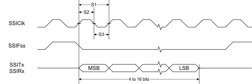
 Figure 5-1 SSI Timing for TI Frame Format (FRF = 01), Single Transfer Timing Measurement
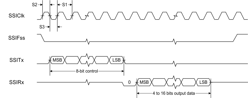
  Figure 5-2 SSI Timing for MICROWIRE Frame Format (FRF = 10), Single Transfer
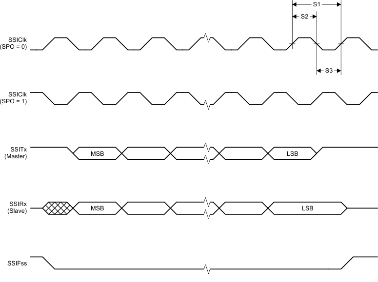
  Figure 5-3 SSI Timing for SPI Frame Format (FRF = 00), With SPH = 1