ZHCSCU4 June 2014 CC2541-Q1
PRODUCTION DATA.
- 1器件概述
- 2修订历史记录
- 3Terminal Configuration and Functions
-
4Specifications
- 4.1 Absolute Maximum Ratings
- 4.2 Handling Ratings
- 4.3 Recommended Operating Conditions
- 4.4 Thermal Characteristics for RHA Package
- 4.5 Electrical Characteristics
- 4.6 General Characteristics
- 4.7 RF Receive Section
- 4.8 RF Transmit Section
- 4.9 32-MHz Crystal Oscillator
- 4.10 32.768-kHz Crystal Oscillator
- 4.11 32-kHz RC Oscillator
- 4.12 16-MHz RC Oscillator
- 4.13 RSSI Characteristics
- 4.14 Frequency Synthesizer Characteristics
- 4.15 Analog Temperature Sensor
- 4.16 Comparator Characteristics
- 4.17 ADC Characteristics
- 4.18 DC Characteristics
- 4.19 Control Input AC Characteristics
- 4.20 SPI AC Characteristics
- 4.21 Debug Interface AC Characteristics
- 4.22 Timer Inputs AC Characteristics
- 4.23 Typical Characteristics
- 5Detailed Description
- 6Application Information
- 7器件和文档支持
- 8机械封装和可订购信息
6 Application Information
Few external components are required for the operation of the CC2541-Q1. A typical application circuit is shown in Figure 6-1.
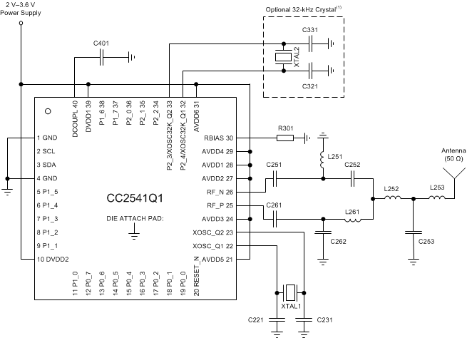
Table 6-1 Overview of External Components (Excluding Supply Decoupling Capacitors)
| Component | Description | Value |
|---|---|---|
| C401 | Decoupling capacitor for the internal 1.8-V digital voltage regulator | 1 µF |
| R301 | Precision resistor ±1%, used for internal biasing | 56 kΩ |
6.1 Input/Output Matching
When using an unbalanced antenna such as a monopole, a balun should be used to optimize performance. The balun can be implemented using low-cost discrete inductors and capacitors. See reference design, CC2541-Q1EM, for recommended balun.
6.2 Crystal
An external 32-MHz crystal, XTAL1, with two loading capacitors (C221 and C231) is used for the 32-MHz crystal oscillator. See Section 4.9 for details. The load capacitance seen by the 32-MHz crystal is given by:
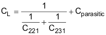
XTAL2 is an optional 32.768-kHz crystal, with two loading capacitors (C321 and C331) used for the 32.768-kHz crystal oscillator. The 32.768-kHz crystal oscillator is used in applications where both very low sleep-current consumption and accurate wake-up times are needed. The load capacitance seen by the 32.768-kHz crystal is given by:

A series resistor may be used to comply with the ESR requirement.
6.3 On-Chip 1.8-V Voltage Regulator Decoupling
The 1.8-V on-chip voltage regulator supplies the 1.8-V digital logic. This regulator requires a decoupling capacitor (C471) for stable operation.
6.4 Power-Supply Decoupling and Filtering
Proper power-supply decoupling must be used for optimum performance. The placement and size of the decoupling capacitors and the power supply filtering are very important to achieve the best performance in an application. TI provides a compact reference design that should be followed very closely.