ZHCSCU4 June 2014 CC2541-Q1
PRODUCTION DATA.
- 1器件概述
- 2修订历史记录
- 3Terminal Configuration and Functions
-
4Specifications
- 4.1 Absolute Maximum Ratings
- 4.2 Handling Ratings
- 4.3 Recommended Operating Conditions
- 4.4 Thermal Characteristics for RHA Package
- 4.5 Electrical Characteristics
- 4.6 General Characteristics
- 4.7 RF Receive Section
- 4.8 RF Transmit Section
- 4.9 32-MHz Crystal Oscillator
- 4.10 32.768-kHz Crystal Oscillator
- 4.11 32-kHz RC Oscillator
- 4.12 16-MHz RC Oscillator
- 4.13 RSSI Characteristics
- 4.14 Frequency Synthesizer Characteristics
- 4.15 Analog Temperature Sensor
- 4.16 Comparator Characteristics
- 4.17 ADC Characteristics
- 4.18 DC Characteristics
- 4.19 Control Input AC Characteristics
- 4.20 SPI AC Characteristics
- 4.21 Debug Interface AC Characteristics
- 4.22 Timer Inputs AC Characteristics
- 4.23 Typical Characteristics
- 5Detailed Description
- 6Application Information
- 7器件和文档支持
- 8机械封装和可订购信息
4 Specifications
4.1 Absolute Maximum Ratings(1)
over operating free-air temperature range (unless otherwise noted)| MIN | MAX | UNIT | ||
|---|---|---|---|---|
| Supply voltage | All supply pins must have the same voltage | –0.3 | 3.9 | V |
| Voltage on any digital pin | –0.3 | VDD + 0.3 ≤ 3.9 | V | |
| Input RF level | 10 | dBm | ||
(1) Stresses beyond those listed under Absolute Maximum Ratings may cause permanent damage to the device. These are stress ratings only, and functional operation of the device at these or any other conditions beyond those indicated under Recommended Operating Conditions is not implied. Exposure to absolute-maximum-rated conditions for extended periods may affect device reliability.
4.2 Handling Ratings
| MIN | MAX | UNIT | ||||
|---|---|---|---|---|---|---|
| Tstg | Storage temperature range | –40 | 125 | °C | ||
| VESD | Electrostatic discharge (ESD) performance: | Human Body Model (HBM), per AEC Q100-002(1) | All pins | –1 | 1 | kV |
| All pins (Excluding pins 25 and 26) |
–2 | 2 | ||||
| Charged Device Model (CDM), per AEC Q100-011 | –500 | 500 | V | |||
(1) AEC Q100-002 indicates HBM stressing is done in accordance with the ANSI/ESDA/JEDEC JS-001 specification.
4.3 Recommended Operating Conditions
over operating free-air temperature range (unless otherwise noted)| MIN | NOM | MAX | UNIT | |
|---|---|---|---|---|
| Operating ambient temperature range, TA | –40 | 105 | °C | |
| Operating supply voltage | 2 | 3.6 | V |
4.4 Thermal Characteristics for RHA Package
| NAME | DESCRIPTION | °C/W | AIR FLOW (m/s)(1) |
|---|---|---|---|
| RΘJC | Junction-to-case (top) | 16.1 | 0.00 |
| RΘJB | Junction-to-board | 5.5 | 0.00 |
| RΘJA | Junction-to-free air | 30.6 | 0.00 |
| PsiJT | Junction-to-package top | 0.2 | 0.00 |
| PsiJB | Junction-to-board | 5.4 | 0.00 |
| RθJC | Junction-to-case (bottom) | 1.0 | 0.00 |
(1) m/s = meters per second
4.5 Electrical Characteristics
Measured on Texas Instruments CC2541-Q1 EM reference design with TA = 25°C and VDD = 3 V,1 Mbps, GFSK, 250-kHz deviation, Bluetooth low energy mode, and 0.1% BER
| PARAMETER | TEST CONDITIONS | MIN | TYP | MAX | UNIT | |
|---|---|---|---|---|---|---|
| Icore | Core current consumption | RX mode, standard mode, no peripherals active, low MCU activity | 18.3 | mA | ||
| RX mode, high-gain mode, no peripherals active, low MCU activity | 20.8 | |||||
| TX mode, –20 dBm output power, no peripherals active, low MCU activity | 17.2 | |||||
| TX mode, 0 dBm output power, no peripherals active, low MCU activity | 18.6 | |||||
| Power mode 1. Digital regulator on; 16-MHz RCOSC and 32-MHz crystal oscillator off; 32.768-kHz XOSC, POR, BOD and sleep timer active; RAM and register retention | 270 | µA | ||||
| Power mode 2. Digital regulator off; 16-MHz RCOSC and 32-MHz crystal oscillator off; 32.768-kHz XOSC, POR, and sleep timer active; RAM and register retention | 1 | |||||
| Power mode 3. Digital regulator off; no clocks; POR active; RAM and register retention | 0.5 | |||||
| Low MCU activity: 32-MHz XOSC running. No radio or peripherals. Limited flash access, no RAM access. | 6.7 | mA | ||||
| Iperi | Peripheral current consumption (Adds to core current Icore for each peripheral unit activated) | Timer 1. Timer running, 32-MHz XOSC used | 90 | μA | ||
| Timer 2. Timer running, 32-MHz XOSC used | 90 | |||||
| Timer 3. Timer running, 32-MHz XOSC used | 60 | |||||
| Timer 4. Timer running, 32-MHz XOSC used | 70 | |||||
| Sleep timer, including 32.753-kHz RCOSC | 0.6 | |||||
| ADC, when converting | 1.2 | mA | ||||
4.6 General Characteristics
Measured on Texas Instruments CC2541-Q1 EM reference design with TA = 25°C and VDD = 3 V| PARAMETER | TEST CONDITIONS | MIN | TYP | MAX | UNIT |
|---|---|---|---|---|---|
| WAKE-UP AND TIMING | |||||
| Power mode 1 → Active | Digital regulator on, 16-MHz RCOSC and 32-MHz crystal oscillator off. Start-up of 16-MHz RCOSC | 4 | μs | ||
| Power mode 2 or 3 → Active | Digital regulator off, 16-MHz RCOSC and 32-MHz crystal oscillator off. Start-up of regulator and 16-MHz RCOSC | 120 | μs | ||
| Active → TX or RX | Crystal ESR = 16 Ω. Initially running on 16-MHz RCOSC, with 32-MHz XOSC OFF | 500 | μs | ||
| With 32-MHz XOSC initially on | 180 | μs | |||
| RX/TX turnaround | Proprietary auto mode | 130 | μs | ||
| BLE mode | 150 | ||||
| RADIO PART | |||||
| RF frequency range | Programmable in 1-MHz steps | 2379 | 2496 | MHz | |
| Data rate and modulation format | 2 Mbps, GFSK, 500-kHz deviation 2 Mbps, GFSK, 320-kHz deviation 1 Mbps, GFSK, 250-kHz deviation 1 Mbps, GFSK, 160-kHz deviation 500 kbps, MSK 250 kbps, GFSK, 160-kHz deviation 250 kbps, MSK |
||||
4.7 RF Receive Section
Measured on Texas Instruments CC2541-Q1 EM reference design with TA = 25°C, VDD = 3 V, fc = 2440 MHz| PARAMETER | TEST CONDITIONS | MIN | TYP | MAX | UNIT |
|---|---|---|---|---|---|
| 1 Mbps, GFSK, 250-kHz Deviation, Bluetooth low energy Mode, 0.1% BER | |||||
| Receiver sensitivity(3)(4) | High-gain mode | –94 | dBm | ||
| Standard mode | –88 | ||||
| Saturation(4) | BER < 0.1% | 5 | dBm | ||
| Co-channel rejection(4) | Wanted signal –67 dBm | –6 | dB | ||
| In-band blocking rejection(4) | ±1 MHz offset, 0.1% BER, wanted signal –67 dBm | –2 | dB | ||
| ±2 MHz offset, 0.1% BER, wanted signal –67 dBm | 26 | ||||
| ±3 MHz offset, 0.1% BER, wanted signal –67 dBm | 34 | ||||
| >6 MHz offset, 0.1% BER, wanted signal –67 dBm | 33 | ||||
| Out-of-band blocking rejection(4) | Minimum interferer level < 2 GHz (Wanted signal –67 dBm) | –21 | dBm | ||
| Minimum interferer level [2 GHz, 3 GHz] (Wanted signal –67 dBm) | –27 | ||||
| Minimum interferer level > 3 GHz (Wanted signal –67 dBm) | –8 | ||||
| Intermodulation(4) | Minimum interferer level | –36 | dBm | ||
| Frequency error tolerance(1) | Including both initial tolerance and drift. Sensitivity better than -67dBm, 250 byte payload. BER 0.1% | –250 | 250 | kHz | |
| Symbol rate error tolerance(2) | Maximum packet length. Sensitivity better than –67 dBm, 250 byte payload. BER 0.1% | –80 | 80 | ppm | |
| ALL RATES/FORMATS | |||||
| Spurious emission in RX. Conducted measurement | f < 1 GHz | –67 | dBm | ||
| Spurious emission in RX. Conducted measurement | f > 1 GHz | –57 | dBm | ||
(1) Difference between center frequency of the received RF signal and local oscillator frequency
(2) Difference between incoming symbol rate and the internally generated symbol rate
(3) The receiver sensitivity setting is programmable using a TI BLE stack vendor-specific API command. The default value is standard mode.
(4) Results based on standard-gain mode.
4.8 RF Transmit Section
Measured on Texas Instruments CC2541-Q1 EM reference design with TA = 25°C, VDD = 3 V and fc = 2440 MHz| PARAMETER | TEST CONDITIONS | MIN | TYP | MAX | UNIT |
|---|---|---|---|---|---|
| Output power | Delivered to a single-ended 50-Ω load through a balun using maximum recommended output power setting | 0 | dBm | ||
| Delivered to a single-ended 50-Ω load through a balun using minimum recommended output power setting | –20 | ||||
| Programmable output power range | Delivered to a single-ended 50-Ω load through a balun using minimum recommended output power setting | 20 | dB | ||
| Spurious emission conducted measurement | f < 1 GHz | –52 | dBm | ||
| f > 1 GHz | –48 | dBm | |||
| Suitable for systems targeting compliance with worldwide radio-frequency regulations ETSI EN 300 328 and EN 300 440 Class 2 (Europe), FCC CFR47 Part 15 (US), and ARIB STD-T66 (Japan) | |||||
| Optimum load impedance | Differential impedance as seen from the RF port (RF_P and RF_N) toward the antenna | 70 +j30 | Ω | ||
Designs with antenna connectors that require conducted ETSI compliance at 64 MHz should insert an LC resonator in front of the antenna connector. Use a 1.6-nH inductor in parallel with a 1.8-pF capacitor. Connect both from the signal trace to a good RF ground.
4.9 32-MHz Crystal Oscillator
Measured on Texas Instruments CC2541-Q1 EM reference design with TA = 25°C and VDD = 3 V| PARAMETER | TEST CONDITIONS | MIN | TYP | MAX | UNIT | |
|---|---|---|---|---|---|---|
| Crystal frequency | 32 | MHz | ||||
| Crystal frequency accuracy requirement(1) | –40 | 40 | ppm | |||
| ESR | Equivalent series resistance | 6 | 60 | Ω | ||
| C0 | Crystal shunt capacitance | 1 | 7 | pF | ||
| CL | Crystal load capacitance | 10 | 16 | pF | ||
| Start-up time | 0.25 | ms | ||||
| Power-down guard time | The crystal oscillator must be in power down for a guard time before it is used again. This requirement is valid for all modes of operation. The need for power-down guard time can vary with crystal type and load. | 3 | ms | |||
(1) Including aging and temperature dependency, as specified by [1]
4.10 32.768-kHz Crystal Oscillator
Measured on Texas Instruments CC2541-Q1 EM reference design with TA = 25°C and VDD = 3 V| PARAMETER | TEST CONDITIONS | MIN | TYP | MAX | UNIT | |
|---|---|---|---|---|---|---|
| Crystal frequency | 32.768 | kHz | ||||
| Crystal frequency accuracy requirement(1) | –40 | 40 | ppm | |||
| ESR | Equivalent series resistance | 40 | 130 | kΩ | ||
| C0 | Crystal shunt capacitance | 0.9 | 2 | pF | ||
| CL | Crystal load capacitance | 12 | 16 | pF | ||
| Start-up time | 0.4 | s | ||||
4.11 32-kHz RC Oscillator
Measured on Texas Instruments CC2541-Q1 EM reference design with TA = 25°C and VDD = 3 V.| PARAMETER | TEST CONDITIONS | MIN | TYP | MAX | UNIT |
|---|---|---|---|---|---|
| Calibrated frequency(1) | 32.753 | kHz | |||
| Frequency accuracy after calibration | ±0.2% | ||||
| Temperature coefficient(2) | 0.4 | %/°C | |||
| Supply-voltage coefficient(3) | 3 | %/V | |||
| Calibration time(4) | 2 | ms |
(1) The calibrated 32-kHz RC oscillator frequency is the 32-MHz XTAL frequency divided by 977.
(2) Frequency drift when temperature changes after calibration
(3) Frequency drift when supply voltage changes after calibration
(4) When the 32-kHz RC oscillator is enabled, it is calibrated when a switch from the 16-MHz RC oscillator to the 32-MHz crystal oscillator is performed while SLEEPCMD.OSC32K_CALDIS is set to 0.
4.12 16-MHz RC Oscillator
Measured on Texas Instruments CC2541-Q1 EM reference design with TA = 25°C and VDD = 3 V| PARAMETER | TEST CONDITIONS | MIN | TYP | MAX | UNIT |
|---|---|---|---|---|---|
| Frequency(1) | 16 | MHz | |||
| Uncalibrated frequency accuracy | ±18% | ||||
| Calibrated frequency accuracy | ±0.6% | ||||
| Start-up time | 10 | μs | |||
| Initial calibration time(2) | 50 | μs |
(1) The calibrated 16-MHz RC oscillator frequency is the 32-MHz XTAL frequency divided by 2.
(2) When the 16-MHz RC oscillator is enabled, it is calibrated when a switch from the 16-MHz RC oscillator to the 32-MHz crystal oscillator is performed while SLEEPCMD.OSC_PD is set to 0.
4.13 RSSI Characteristics
Measured on Texas Instruments CC2541-Q1 EM reference design with TA = 25°C and VDD = 3 V| PARAMETER | TEST CONDITIONS | MIN | TYP | MAX | UNIT | ||
|---|---|---|---|---|---|---|---|
| 2 Mbps, GFSK, 320-kHz Deviation, 0.1% BER and 2 Mbps, GFSK, 500-kHz Deviation, 0.1% BER | |||||||
| Useful RSSI range(1) | Reduced gain by AGC algorithm | 64 | dB | ||||
| High gain by AGC algorithm | 64 | ||||||
| RSSI offset(1) | Reduced gain by AGC algorithm | 79 | dBm | ||||
| High gain by AGC algorithm | 99 | ||||||
| Absolute uncalibrated accuracy(1) | ±6 | dB | |||||
| Step size (LSB value) | 1 | dB | |||||
| All Other Rates/Formats | |||||||
| Useful RSSI range(1) | Standard mode | 64 | dB | ||||
| High-gain mode | 64 | ||||||
| RSSI offset(1) | Standard mode | 98 | dBm | ||||
| High-gain mode | 107 | ||||||
| Absolute uncalibrated accuracy(1) | ±3 | dB | |||||
| Step size (LSB value) | 1 | dB | |||||
(1) Assuming CC2541-Q1 EM reference design. Other RF designs give an offset from the reported value.
4.14 Frequency Synthesizer Characteristics
Measured on Texas Instruments CC2541-Q1 EM reference design with TA = 25°C, VDD = 3 V and fc = 2440 MHz| PARAMETER | TEST CONDITIONS | MIN | TYP | MAX | UNIT |
|---|---|---|---|---|---|
| Phase noise, unmodulated carrier | At ±1-MHz offset from carrier | –109 | dBc/Hz | ||
| At ±3-MHz offset from carrier | –112 | ||||
| At ±5-MHz offset from carrier | –119 |
4.15 Analog Temperature Sensor
Measured on Texas Instruments CC2541-Q1 EM reference design with TA = 25°C and VDD = 3 V4.16 Comparator Characteristics
TA = 25°C, VDD = 3 V. All measurement results are obtained using the CC2541-Q1 reference designs, post-calibration.| PARAMETER | TEST CONDITIONS | MIN | TYP | MAX | UNIT | |
|---|---|---|---|---|---|---|
| Common-mode maximum voltage | VDD | V | ||||
| Common-mode minimum voltage | –0.3 | |||||
| Input offset voltage | 1 | mV | ||||
| Offset vs temperature | 16 | µV/°C | ||||
| Offset vs operating voltage | 4 | mV/V | ||||
| Supply current | 230 | nA | ||||
| Hysteresis | 0.15 | mV | ||||
4.17 ADC Characteristics
TA = 25°C and VDD = 3 V| PARAMETER | TEST CONDITIONS | MIN | TYP | MAX | UNIT | |
|---|---|---|---|---|---|---|
| Input voltage | VDD is voltage on AVDD5 pin | 0 | VDD | V | ||
| External reference voltage | VDD is voltage on AVDD5 pin | 0 | VDD | V | ||
| External reference voltage differential | VDD is voltage on AVDD5 pin | 0 | VDD | V | ||
| Input resistance, signal | Simulated using 4-MHz clock speed | 197 | kΩ | |||
| Full-scale signal(1) | Peak-to-peak, defines 0 dBFS | 2.97 | V | |||
| ENOB(1) | Effective number of bits | Single-ended input, 7-bit setting | 5.7 | bits | ||
| Single-ended input, 9-bit setting | 7.5 | |||||
| Single-ended input, 10-bit setting | 9.3 | |||||
| Single-ended input, 12-bit setting | 10.3 | |||||
| Differential input, 7-bit setting | 6.5 | |||||
| Differential input, 9-bit setting | 8.3 | |||||
| Differential input, 10-bit setting | 10 | |||||
| Differential input, 12-bit setting | 11.5 | |||||
| 10-bit setting, clocked by RCOSC | 9.7 | |||||
| 12-bit setting, clocked by RCOSC | 10.9 | |||||
| Useful power bandwidth | 7-bit setting, both single and differential | 0–20 | kHz | |||
| THD | Total harmonic distortion | Single ended input, 12-bit setting, –6 dBFS(1) | –75.2 | dB | ||
| Differential input, 12-bit setting, –6 dBFS(1) | –86.6 | |||||
| Signal to nonharmonic ratio | Single-ended input, 12-bit setting(1) | 70.2 | dB | |||
| Differential input, 12-bit setting(1) | 79.3 | |||||
| Single-ended input, 12-bit setting, –6 dBFS(1) | 78.8 | |||||
| Differential input, 12-bit setting, –6 dBFS(1) | 88.9 | |||||
| CMRR | Common-mode rejection ratio | Differential input, 12-bit setting, 1-kHz sine (0 dBFS), limited by ADC resolution |
>84 | dB | ||
| Crosstalk | Single ended input, 12-bit setting, 1-kHz sine (0 dBFS), limited by ADC resolution |
>84 | dB | |||
| Offset | Midscale | –3 | mV | |||
| Gain error | 0.68% | |||||
| DNL | Differential nonlinearity | 12-bit setting, mean(1) | 0.05 | LSB | ||
| 12-bit setting, maximum(1) | 0.9 | |||||
| INL | Integral nonlinearity | 12-bit setting, mean(1) | 4.6 | LSB | ||
| 12-bit setting, maximum(1) | 13.3 | |||||
| 12-bit setting, mean, clocked by RCOSC | 10 | |||||
| 12-bit setting, max, clocked by RCOSC | 29 | |||||
| SINAD (–THD+N) |
Signal-to-noise-and-distortion | Single ended input, 7-bit setting(1) | 35.4 | dB | ||
| Single ended input, 9-bit setting(1) | 46.8 | |||||
| Single ended input, 10-bit setting(1) | 57.5 | |||||
| Single ended input, 12-bit setting(1) | 66.6 | |||||
| Differential input, 7-bit setting(1) | 40.7 | |||||
| Differential input, 9-bit setting(1) | 51.6 | |||||
| Differential input, 10-bit setting(1) | 61.8 | |||||
| Differential input, 12-bit setting(1) | 70.8 | |||||
| Conversion time | 7-bit setting | 20 | μs | |||
| 9-bit setting | 36 | |||||
| 10-bit setting | 68 | |||||
| 12-bit setting | 132 | |||||
| Power consumption | 1.2 | mA | ||||
| Internal reference VDD coefficient | 4 | mV/V | ||||
| Internal reference temperature coefficient | 0.4 | mV/10°C | ||||
| Internal reference voltage | 1.24 | V | ||||
(1) Measured with 300-Hz sine-wave input and VDD as reference.
4.18 DC Characteristics
TA = 25°C, VDD = 3 V| PARAMETER | TEST CONDITIONS | MIN | TYP | MAX | UNIT |
|---|---|---|---|---|---|
| Logic-0 input voltage | 0.5 | V | |||
| Logic-1 input voltage | 2.4 | V | |||
| Logic-0 input current | Input equals 0 V | –50 | 50 | nA | |
| Logic-1 input current | Input equals VDD | –50 | 50 | nA | |
| I/O-pin pullup and pulldown resistors | 20 | kΩ | |||
| Logic-0 output voltage, 4- mA pins | Output load 4 mA | 0.5 | V | ||
| Logic-1 output voltage, 4-mA pins | Output load 4 mA | 2.5 | V | ||
| Logic-0 output voltage, 20- mA pins | Output load 20 mA | 0.5 | V | ||
| Logic-1 output voltage, 20-mA pins | Output load 20 mA | 2.5 | V |
4.19 Control Input AC Characteristics
TA = –40°C to 105°C, VDD = 2 V to 3.6 V| PARAMETER | TEST CONDITIONS | MIN | TYP | MAX | UNIT |
|---|---|---|---|---|---|
| System clock, fSYSCLK
tSYSCLK = 1/ fSYSCLK |
The undivided system clock is 32 MHz when crystal oscillator is used. The undivided system clock is 16 MHz when calibrated 16-MHz RC oscillator is used. | 16 | 32 | MHz | |
| RESET_N low duration | See item 1, Figure 4-1. This is the shortest pulse that is recognized as a complete reset pin request. Note that shorter pulses may be recognized but do not lead to complete reset of all modules within the chip. | 1 | µs | ||
| Interrupt pulse duration | See item 2, Figure 4-1.This is the shortest pulse that is recognized as an interrupt request. | 20 | ns |
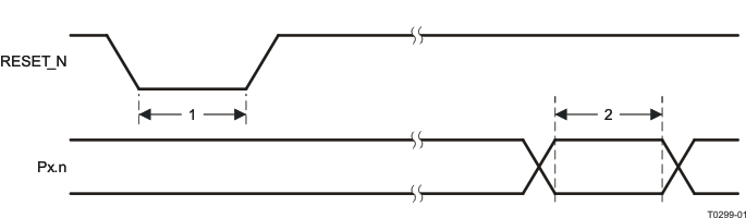 Figure 4-1 Control Input AC Characteristics
4.20 SPI AC Characteristics
TA = –40°C to 105°C, VDD = 2 V to 3.6 V| PARAMETER | TEST CONDITIONS | MIN | TYP | MAX | UNIT | |
|---|---|---|---|---|---|---|
| t1 | SCK period | Master, RX and TX | 250 | ns | ||
| Slave, RX and TX | 250 | |||||
| SCK duty cycle | Master | 50% | ||||
| t2 | SSN low to SCK | Master | 63 | ns | ||
| Slave | 63 | |||||
| t3 | SCK to SSN high | Master | 63 | ns | ||
| Slave | 63 | |||||
| t4 | MOSI early out | Master, load = 10 pF | 7 | ns | ||
| t5 | MOSI late out | Master, load = 10 pF | 10 | ns | ||
| t6 | MISO setup | Master | 90 | ns | ||
| t7 | MISO hold | Master | 10 | ns | ||
| SCK duty cycle | Slave | 50% | ns | |||
| t10 | MOSI setup | Slave | 35 | ns | ||
| t11 | MOSI hold | Slave | 10 | ns | ||
| t9 | MISO late out | Slave, load = 10 pF | 95 | ns | ||
| Operating frequency | Master, TX only | 8 | MHz | |||
| Master, RX and TX | 4 | |||||
| Slave, RX only | 8 | |||||
| Slave, RX and TX | 4 | |||||
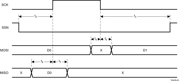 Figure 4-2 SPI Master AC Characteristics
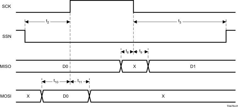 Figure 4-3 SPI Slave AC Characteristics
4.21 Debug Interface AC Characteristics
TA = –40°C to 105°C, VDD = 2 V to 3.6 V| PARAMETER | TEST CONDITIONS | MIN | TYP | MAX | UNIT | |
|---|---|---|---|---|---|---|
| fclk_dbg | Debug clock frequency (see Figure 4-4) | 12 | MHz | |||
| t1 | Allowed high pulse on clock (see Figure 4-4) | 35 | ns | |||
| t2 | Allowed low pulse on clock (see Figure 4-4) | 35 | ns | |||
| t3 | EXT_RESET_N low to first falling edge on debug clock (see Figure 4-6) | 167 | ns | |||
| t4 | Falling edge on clock to EXT_RESET_N high (see Figure 4-6) | 83 | ns | |||
| t5 | EXT_RESET_N high to first debug command (see Figure 4-6) | 83 | ns | |||
| t6 | Debug data setup (see Figure 4-5) | 2 | ns | |||
| t7 | Debug data hold (see Figure 4-5) | 4 | ns | |||
| t8 | Clock-to-data delay (see Figure 4-5) | Load = 10 pF | 30 | ns | ||
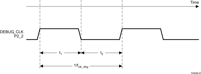 Figure 4-4 Debug Clock – Basic Timing
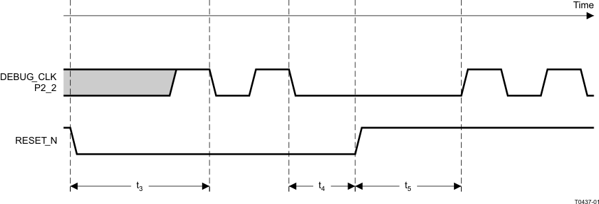 Figure 4-5 Debug Enable Timing
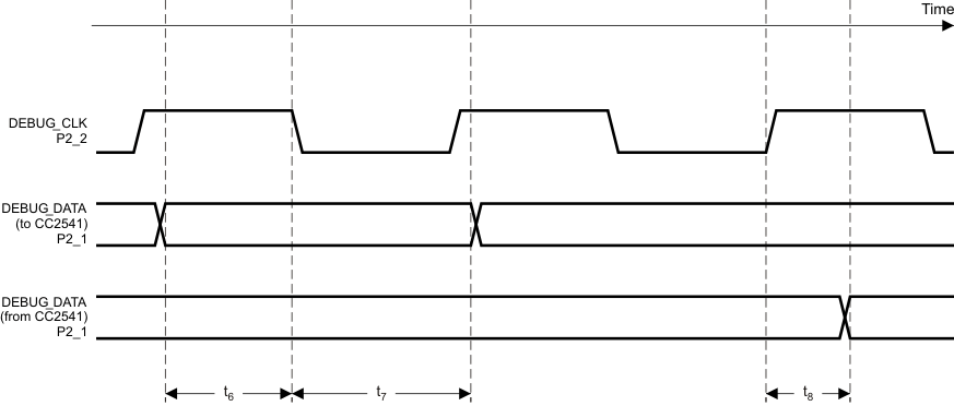 Figure 4-6 Data Setup and Hold Timing
4.22 Timer Inputs AC Characteristics
TA = –40°C to 105°C, VDD = 2 V to 3.6 V| PARAMETER | TEST CONDITIONS | MIN | TYP | MAX | UNIT |
|---|---|---|---|---|---|
| Input capture pulse duration | Synchronizers determine the shortest input pulse that can be recognized. The synchronizers operate at the current system clock rate (16 MHz or 32 MHz). | 1.5 | tSYSCLK |
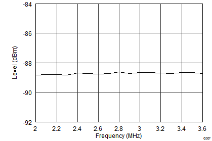
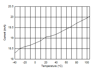
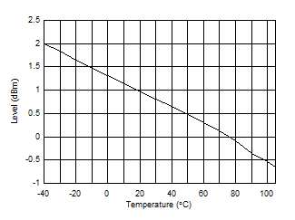
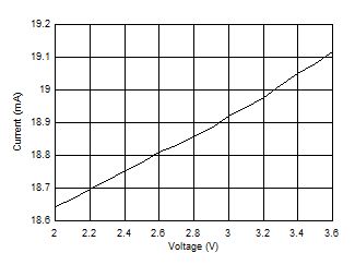
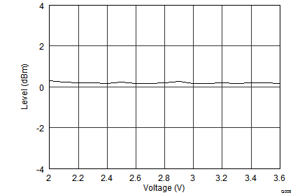
4.23 Typical Characteristics
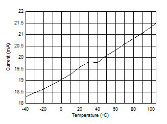
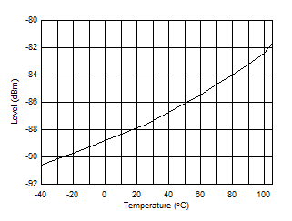
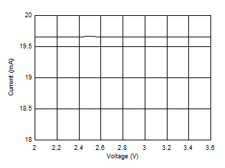
| 1-Mbps GFSK 250-kHz Standard Gain Setting | ||
| TA = 25°C |
| 1-Mbps GFSK 250-kHz Standard Gain Setting | ||
| TA = 25°C | ||
| Vcc = 3 V |
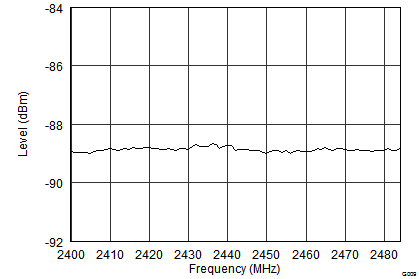
| TX Power Setting = 0 dBm | ||
| TA = 25°C |
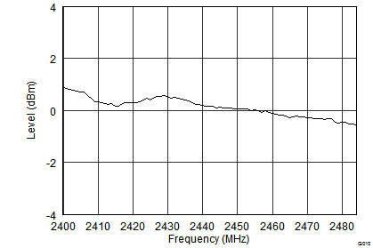
| TX Power Setting = 0 dBm | ||
| TA = 25°C | ||
| Vcc = 3 V |
Table 4-1 Output Power(1)(2)
| TX POWER Setting | Typical Output Power (dBm) |
|---|---|
| 0xE1 | 0 |
| 0xD1 | –2 |
| 0xC1 | –4 |
| 0xB1 | –6 |
| 0xA1 | –8 |
| 0x91 | –10 |
| 0x81 | –12 |
| 0x71 | –14 |
| 0x61 | –16 |
| 0x51 | –18 |
| 0x41 | –20 |
(1) Measured on Texas Instruments CC2541-Q1 EM reference design with TA = 25°C, VDD = 3 V and fc = 2440 MHz. See SWRU191 for recommended register settings.
(2) 1 Mbsp, GFSK, 250-kHz deviation, Bluetooth low energy mode, 1% BER