ZHCSCU4 June 2014 CC2541-Q1
PRODUCTION DATA.
- 1器件概述
- 2修订历史记录
- 3Terminal Configuration and Functions
-
4Specifications
- 4.1 Absolute Maximum Ratings
- 4.2 Handling Ratings
- 4.3 Recommended Operating Conditions
- 4.4 Thermal Characteristics for RHA Package
- 4.5 Electrical Characteristics
- 4.6 General Characteristics
- 4.7 RF Receive Section
- 4.8 RF Transmit Section
- 4.9 32-MHz Crystal Oscillator
- 4.10 32.768-kHz Crystal Oscillator
- 4.11 32-kHz RC Oscillator
- 4.12 16-MHz RC Oscillator
- 4.13 RSSI Characteristics
- 4.14 Frequency Synthesizer Characteristics
- 4.15 Analog Temperature Sensor
- 4.16 Comparator Characteristics
- 4.17 ADC Characteristics
- 4.18 DC Characteristics
- 4.19 Control Input AC Characteristics
- 4.20 SPI AC Characteristics
- 4.21 Debug Interface AC Characteristics
- 4.22 Timer Inputs AC Characteristics
- 4.23 Typical Characteristics
- 5Detailed Description
- 6Application Information
- 7器件和文档支持
- 8机械封装和可订购信息
3 Terminal Configuration and Functions
The CC2541-Q1 pinout is shown in Figure 3-1 and a short description of the pins follows.
3.1 Pin Diagram
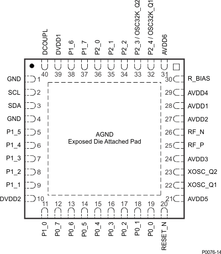
The exposed ground pad must be connected to a solid ground plane, as this is the ground connection for the chip.
Figure 3-1 RHA PACKAGE (TOP VIEW)
3.2 Pin Descriptions
Table 3-1 Pin Descriptions
| PINS | TYPE | DESCRIPTION | |
|---|---|---|---|
| NAME | NO. | ||
| AVDD1 | 28 | Power (analog) | 2-V–3.6-V analog power-supply connection |
| AVDD2 | 27 | Power (analog) | 2-V–3.6-V analog power-supply connection |
| AVDD3 | 24 | Power (analog) | 2-V–3.6-V analog power-supply connection |
| AVDD4 | 29 | Power (analog) | 2-V–3.6-V analog power-supply connection |
| AVDD5 | 21 | Power (analog) | 2-V–3.6-V analog power-supply connection |
| AVDD6 | 31 | Power (analog) | 2-V–3.6-V analog power-supply connection |
| DCOUPL | 40 | Power (digital) | 1.8-V digital power-supply decoupling. Do not use for supplying external circuits. |
| DVDD1 | 39 | Power (digital) | 2-V–3.6-V digital power-supply connection |
| DVDD2 | 10 | Power (digital) | 2-V–3.6-V digital power-supply connection |
| GND | 1 | Ground pin | Connect to GND |
| GND | — | Ground | The ground pad must be connected to a solid ground plane. |
| GND | 4 | Ground pin | Connect to GND |
| P0_0 | 19 | Digital I/O | Port 0.0 |
| P0_1 | 18 | Digital I/O | Port 0.1 |
| P0_2 | 17 | Digital I/O | Port 0.2 |
| P0_3 | 16 | Digital I/O | Port 0.3 |
| P0_4 | 15 | Digital I/O | Port 0.4 |
| P0_5 | 14 | Digital I/O | Port 0.5 |
| P0_6 | 13 | Digital I/O | Port 0.6 |
| P0_7 | 12 | Digital I/O | Port 0.7 |
| P1_0 | 11 | Digital I/O | Port 1.0 – 20-mA drive capability |
| P1_1 | 9 | Digital I/O | Port 1.1 – 20-mA drive capability |
| P1_2 | 8 | Digital I/O | Port 1.2 |
| P1_3 | 7 | Digital I/O | Port 1.3 |
| P1_4 | 6 | Digital I/O | Port 1.4 |
| P1_5 | 5 | Digital I/O | Port 1.5 |
| P1_6 | 38 | Digital I/O | Port 1.6 |
| P1_7 | 37 | Digital I/O | Port 1.7 |
| P2_0 | 36 | Digital I/O | Port 2.0 |
| P2_1/DD | 35 | Digital I/O | Port 2.1 / debug data |
| P2_2/DC | 34 | Digital I/O | Port 2.2 / debug clock |
| P2_3/ OSC32K_Q2 | 33 | Digital I/O, Analog I/O | Port 2.3/32.768 kHz XOSC |
| P2_4/ OSC32K_Q1 | 32 | Digital I/O, Analog I/O | Port 2.4/32.768 kHz XOSC |
| RBIAS | 30 | Analog I/O | External precision bias resistor for reference current |
| RESET_N | 20 | Digital input | Reset, active-low |
| RF_N | 26 | RF I/O | Negative RF input signal to LNA during RX Negative RF output signal from PA during TX |
| RF_P | 25 | RF I/O | Positive RF input signal to LNA during RX Positive RF output signal from PA during TX |
| SCL | 2 | I2C clock or digital I/O | Can be used as I2C clock pin or digital I/O. Leave floating if not used. If grounded disable pull up |
| SDA | 3 | I2C clock or digital I/O | Can be used as I2C data pin or digital I/O. Leave floating if not used. If grounded disable pull up |
| XOSC_Q1 | 22 | Analog I/O | 32-MHz crystal oscillator pin 1 or external clock input |
| XOSC_Q2 | 23 | Analog I/O | 32-MHz crystal oscillator pin 2 |