ZHCSCU4 June 2014 CC2541-Q1
PRODUCTION DATA.
- 1器件概述
- 2修订历史记录
- 3Terminal Configuration and Functions
-
4Specifications
- 4.1 Absolute Maximum Ratings
- 4.2 Handling Ratings
- 4.3 Recommended Operating Conditions
- 4.4 Thermal Characteristics for RHA Package
- 4.5 Electrical Characteristics
- 4.6 General Characteristics
- 4.7 RF Receive Section
- 4.8 RF Transmit Section
- 4.9 32-MHz Crystal Oscillator
- 4.10 32.768-kHz Crystal Oscillator
- 4.11 32-kHz RC Oscillator
- 4.12 16-MHz RC Oscillator
- 4.13 RSSI Characteristics
- 4.14 Frequency Synthesizer Characteristics
- 4.15 Analog Temperature Sensor
- 4.16 Comparator Characteristics
- 4.17 ADC Characteristics
- 4.18 DC Characteristics
- 4.19 Control Input AC Characteristics
- 4.20 SPI AC Characteristics
- 4.21 Debug Interface AC Characteristics
- 4.22 Timer Inputs AC Characteristics
- 4.23 Typical Characteristics
- 5Detailed Description
- 6Application Information
- 7器件和文档支持
- 8机械封装和可订购信息
5 Detailed Description
5.1 Functional Block Diagram
A block diagram of the CC2541-Q1 is shown in Figure 5-1. The modules can be roughly divided into one of three categories: CPU-related modules; modules related to power, test, and clock distribution; and radio-related modules. In the following subsections, a short description of each module is given.
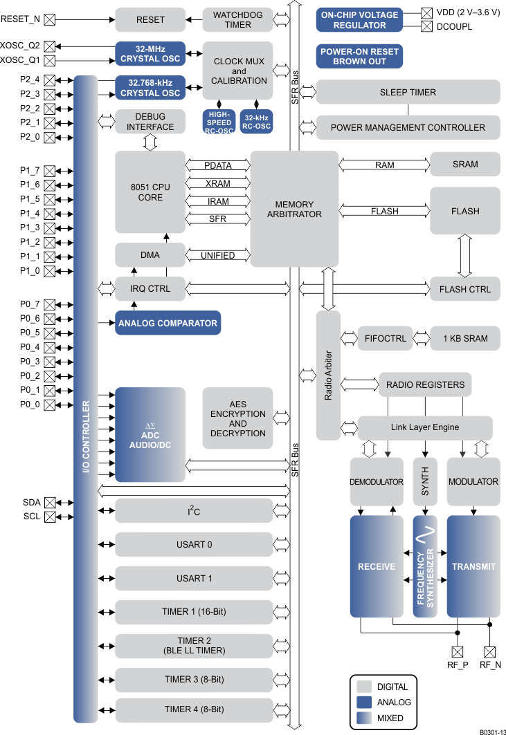 Figure 5-1 CC2541-Q1 Block Diagram
5.2 Block Descriptions
A block diagram of the CC2541-Q1 is shown in Figure 5-1. The modules can be roughly divided into one of three categories: CPU-related modules; modules related to power, test, and clock distribution; and radio-related modules. In the following subsections, a short description of each module is given.
5.2.1 CPU and Memory
The 8051 CPU core is a single-cycle 8051-compatible core. It has three different memory access busses (SFR, DATA, and CODE/XDATA), a debug interface, and an 18-input extended interrupt unit.
The memory arbiter is at the heart of the system, as it connects the CPU and DMA controller with the physical memories and all peripherals through the SFR bus. The memory arbiter has four memory-access points, access of which can map to one of three physical memories: an SRAM, flash memory, and XREG/SFR registers. It is responsible for performing arbitration and sequencing between simultaneous memory accesses to the same physical memory.
The SFR bus is drawn conceptually in Figure 5-1 as a common bus that connects all hardware peripherals to the memory arbiter. The SFR bus in the block diagram also provides access to the radio registers in the radio register bank, even though these are indeed mapped into XDATA memory space.
The 8-KB SRAM maps to the DATA memory space and to parts of the XDATA memory spaces. The SRAM is an ultralow-power SRAM that retains its contents even when the digital part is powered off (power mode 2 and mode 3).
The 256 KB flash block provides in-circuit programmable non-volatile program memory for the device, and maps into the CODE and XDATA memory spaces.
5.2.2 Peripherals
Writing to the flash block is performed through a flash controller that allows page-wise erasure and 4-bytewise programming. See User Guide for details on the flash controller.
A versatile five-channel DMA controller is available in the system, accesses memory using the XDATA memory space, and thus has access to all physical memories. Each channel (trigger, priority, transfer mode, addressing mode, source and destination pointers, and transfer count) is configured with DMA descriptors that can be located anywhere in memory. Many of the hardware peripherals (AES core, flash controller, USARTs, timers, ADC interface, etc.) can be used with the DMA controller for efficient operation by performing data transfers between a single SFR or XREG address and flash/SRAM.
Each CC2541-Q1 contains a unique 48-bit IEEE address that can be used as the public device address for a Bluetooth device. Designers are free to use this address, or provide their own, as described in the Bluetooth specfication.
The interrupt controller services a total of 18 interrupt sources, divided into six interrupt groups, each of which is associated with one of four interrupt priorities. I/O and sleep timer interrupt requests are serviced even if the device is in a sleep mode (power modes 1 and 2) by bringing the CC2541-Q1 back to the active mode.
The debug interface implements a proprietary two-wire serial interface that is used for in-circuit debugging. Through this debug interface, it is possible to erase or program the entire flash memory, control which oscillators are enabled, stop and start execution of the user program, execute instructions on the 8051 core, set code breakpoints, and single-step through instructions in the code. Using these techniques, it is possible to perform in-circuit debugging and external flash programming elegantly.
The I/O controller is responsible for all general-purpose I/O pins. The CPU can configure whether peripheral modules control certain pins or whether they are under software control, and if so, whether each pin is configured as an input or output and if a pullup or pulldown resistor in the pad is connected. Each peripheral that connects to the I/O pins can choose between two different I/O pin locations to ensure flexibility in various applications.
The sleep timer is an ultralow-power timer that can either use an external 32.768-kHz crystal oscillator or an internal 32.753-kHz RC oscillator. The sleep timer runs continuously in all operating modes except power mode 3. Typical applications of this timer are as a real-time counter or as a wake-up timer to get out of power mode 1 or mode 2.
A built-in watchdog timer allows the CC2541-Q1 to reset itself if the firmware hangs. When enabled by software, the watchdog timer must be cleared periodically; otherwise, it resets the device when it times out.
Timer 1 is a 16-bit timer with timer/counter/PWM functionality. It has a programmable prescaler, a 16-bit period value, and five individually programmable counter/capture channels, each with a 16-bit compare value. Each of the counter/capture channels can be used as a PWM output or to capture the timing of edges on input signals. It can also be configured in IR generation mode, where it counts timer 3 periods and the output is ANDed with the output of timer 3 to generate modulated consumer IR signals with minimal CPU interaction.
Timer 2 is a 40-bit timer. It has a 16-bit counter with a configurable timer period and a 24-bit overflow counter that can be used to keep track of the number of periods that have transpired. A 40-bit capture register is also used to record the exact time at which a start-of-frame delimiter is received/transmitted or the exact time at which transmission ends. There are two 16-bit output compare registers and two 24-bit overflow compare registers that can be used to give exact timing for start of RX or TX to the radio or general interrupts.
Timer 3 and timer 4 are 8-bit timers with timer/counter/PWM functionality. They have a programmable prescaler, an 8-bit period value, and one programmable counter channel with an 8-bit compare value. Each of the counter channels can be used as PWM output.
USART 0 and USART 1 are each configurable as either an SPI master/slave or a UART. They provide double buffering on both RX and TX and hardware flow control and are thus well suited to high-throughput full-duplex applications. Each USART has its own high-precision baud-rate generator, thus leaving the ordinary timers free for other uses. When configured as SPI slaves, the USARTs sample the input signal using SCK directly instead of using some oversampling scheme, and are thus well-suited for high data rates.
The AES encryption/decryption core allows the user to encrypt and decrypt data using the AES algorithm with 128-bit keys. The AES core also supports ECB, CBC, CFB, OFB, CTR, and CBC-MAC, as well as hardware support for CCM.
The ADC supports 7 to 12 bits of resolution with a corresponding range of bandwidths from 30-kHz to 4-kHz, respectively. DC and audio conversions with up to eight input channels (I/O controller pins) are possible. The inputs can be selected as single-ended or differential. The reference voltage can be internal, AVDD, or a single-ended or differential external signal. The ADC also has a temperature-sensor input channel. The ADC can automate the process of periodic sampling or conversion over a sequence of channels.
The I2C module provides a digital peripheral connection with two pins and supports both master and slave operation. I2C support is compliant with the NXP I2C specification version 2.1 and supports standard mode (up to 100 kbps) and fast mode (up to 400 kbps). In addition, 7-bit device addressing modes are supported, as well as master and slave modes.
The ultralow-power analog comparator enables applications to wake up from PM2 or PM3 based on an analog signal. Both inputs are brought out to pins; the reference voltage must be provided externally. The comparator output is connected to the I/O controller interrupt detector and can be treated by the MCU as a regular I/O pin interrupt.