ZHCSEJ8B January 2011 – December 2015
PRODUCTION DATA.
- 1 特性
- 2 应用
- 3 说明
- 4 修订历史记录
- 5 说明 (续)
- 6 Pin Configuration and Functions
-
7 Specifications
- 7.1 Absolute Maximum Ratings
- 7.2 ESD Ratings
- 7.3 Recommended Operating Conditions
- 7.4 Thermal Information
- 7.5 Electrical Characteristics: General Purpose I/O
- 7.6 Supply Current
- 7.7 REG27 LDO
- 7.8 Coulomb Counter
- 7.9 ADC
- 7.10 External Capacitor Voltage Balance Drive
- 7.11 Capacitor Voltage Monitor
- 7.12 Internal Temperature Sensor
- 7.13 Thermistor Measurement Support
- 7.14 Internal Thermal Shutdown
- 7.15 High-Frequency Oscillator
- 7.16 Low-Frequency Oscillator
- 7.17 RAM Backup
- 7.18 Flash
- 7.19 Current Protection Thresholds
- 7.20 Current Protection Timing
- 7.21 Timing Requirements: SMBus
- 7.22 Typical Characteristics
-
8 Detailed Description
- 8.1 Overview
- 8.2 Functional Block Diagram
- 8.3
Feature Description
- 8.3.1 Capacitance Monitoring and Learning
- 8.3.2 Capacitor Voltage Balancing
- 8.3.3 Charge Control
- 8.3.4 Lifetime Data Gathering
- 8.3.5
Safety Detection Features
- 8.3.5.1 Capacitor Overvoltage (OV)
- 8.3.5.2 Capacitor Voltage Imbalance (CIM)
- 8.3.5.3 Weak Capacitor (CLBAD)
- 8.3.5.4 Overtemperature (OT)
- 8.3.5.5 Overcurrent During Charging (OC Chg)
- 8.3.5.6 Overcurrent During Discharging (OC Dsg)
- 8.3.5.7 Short-Circuit During Charging (SC Chg)
- 8.3.5.8 Short-Circuit During Discharging (SC Dsg)
- 8.3.5.9 AFE Watchdog (WDF)
- 8.3.5.10 Integrated AFE Communication Fault (AFE_C)
- 8.3.5.11 Data Flash Fault (DFF)
- 8.3.5.12 FAULT Indication (FAULT Pin)
- 8.3.6 Communications
- 8.3.7 Security (Enables and Disables Features)
- 8.3.8
Measurement System Calibration
- 8.3.8.1 Coulomb Counter Deadband
- 8.3.8.2 Auto Calibration
- 8.3.8.3 Current Gain
- 8.3.8.4 CC Delta
- 8.3.8.5 Cap1 K-factor
- 8.3.8.6 Cap2 K-factor
- 8.3.8.7 Cap3 K-factor
- 8.3.8.8 Cap4 K-factor
- 8.3.8.9 Cap5 K-factor
- 8.3.8.10 K-factor Override Flag
- 8.3.8.11 System Voltage K-factor
- 8.3.8.12 Stack Voltage K-factor
- 8.3.8.13 K-factor Stack Override Flag
- 8.3.8.14 CC Offset
- 8.3.8.15 Board Offset
- 8.3.8.16 Int Temp Offset
- 8.3.8.17 Ext1 Temp Offset
- 8.3.8.18 CC Current
- 8.3.8.19 Voltage Signal
- 8.3.8.20 Temp Signal
- 8.3.8.21 CC Offset Time
- 8.3.8.22 ADC Offset Time
- 8.3.8.23 Current Gain Time
- 8.3.8.24 Voltage Time
- 8.3.8.25 Temperature Time
- 8.3.8.26 Cal Mode Timeout
- 8.3.8.27 Ext Coef a1..a5, b1..b4, Ext rc0, Ext adc0
- 8.3.8.28 Rpad
- 8.3.8.29 Rint
- 8.3.8.30 Int Coef 1..4, Int Min AD, Int Max Temp
- 8.3.8.31 Filter
- 8.3.8.32 Deadband
- 8.3.8.33 CC Deadband
- 8.4 Device Functional Modes
- 8.5
Programming
- 8.5.1 Communications
- 8.5.2
SBS Commands
- 8.5.2.1 SBS Command Summary
- 8.5.2.2
SBS Command Details
- 8.5.2.2.1
ManufacturerAccess (0x00)
- 8.5.2.2.1.1 Device Type (0x0001)
- 8.5.2.2.1.2 Firmware Version (0x0002)
- 8.5.2.2.1.3 Hardware Version (0x0003)
- 8.5.2.2.1.4 DF Checksum (0x0004)
- 8.5.2.2.1.5 Seal Device (0x0020)
- 8.5.2.2.1.6 Lifetime and Capacitor Balancing Enable (0x0021)
- 8.5.2.2.1.7 FAULT Activation (0x0030)
- 8.5.2.2.1.8 FAULT Clear (0x0031)
- 8.5.2.2.1.9 CHGLVL0 Activation (0x0032)
- 8.5.2.2.1.10 CHGLVL0 Clear (0x0033)
- 8.5.2.2.1.11 CHGLVL1 Activation (0x0033)
- 8.5.2.2.1.12 CHGLVL1 Clear (0x0034)
- 8.5.2.2.1.13 Learn Load Activation (0x0037)
- 8.5.2.2.1.14 Learn Load Clear (0x0038)
- 8.5.2.2.1.15 Calibration Mode (0x0040)
- 8.5.2.2.1.16 Reset (0x0041)
- 8.5.2.2.1.17 Unseal Device (UnsealKey)
- 8.5.2.2.1.18 Extended SBS Commands
- 8.5.2.2.2 Temperature (0x08)
- 8.5.2.2.3 Voltage (0x09)
- 8.5.2.2.4 Current (0x0a)
- 8.5.2.2.5 ESR (0x0b)
- 8.5.2.2.6 RelativeStateofCharge (0x0d)
- 8.5.2.2.7 Health (0x0e)
- 8.5.2.2.8 Capacitance (0x10)
- 8.5.2.2.9 ChargingCurrent (0x14)
- 8.5.2.2.10 ChargingVoltage (0x15)
- 8.5.2.2.11 CapacitorVoltage5..1 (0x3b..0x3f)
- 8.5.2.2.12 Extended SBS Commands
- 8.5.2.2.1
ManufacturerAccess (0x00)
- 8.5.3
Data Flash
- 8.5.3.1 Accessing Data Flash
- 8.5.3.2 Data Flash Interface
- 8.5.3.3 Data Flash Summary
- 8.5.3.4
Specific Data Flash Programming Details
- 8.5.3.4.1 OC Dsg
- 8.5.3.4.2 OC Dsg Time
- 8.5.3.4.3 SC Dsg Cfg
- 8.5.3.4.4 SC Chg Cfg
- 8.5.3.4.5 Initial Full Charge Capacitance
- 8.5.3.4.6 Full Charge Capacitance
- 8.5.3.4.7 Firmware Version
- 8.5.3.4.8 Hardware Revision
- 8.5.3.4.9 Manuf. Info
- 8.5.3.4.10 Operation Cfg
- 8.5.3.4.11 FET ACTION
- 8.5.3.4.12 FAULT
- 8.5.3.4.13 AFE State_CTL
- 8.5.3.4.14 Measurement Margin %
- 8.5.3.4.15 Timer
- 8.5.3.4.16 V Chg Nominal
- 8.5.3.4.17 V Chg A
- 8.5.3.4.18 V Chg B
- 8.5.3.4.19 V Chg Max
- 8.5.3.4.20 Min Voltage
- 8.5.3.4.21 Learning Frequency
- 8.5.3.4.22 Dsg Current Threshold
- 8.5.3.4.23 Chg Current Threshold
- 8.5.3.4.24 Quit Current
- 9 Application and Implementation
- 10Power Supply Recommendations
- 11Layout
- 12器件和文档支持
- 13机械、封装和可订购信息
9 Application and Implementation
NOTE
Information in the following applications sections is not part of the TI component specification, and TI does not warrant its accuracy or completeness. TI’s customers are responsible for determining suitability of components for their purposes. Customers should validate and test their design implementation to confirm system functionality.
9.1 Application Information
The bq33100 is a super capacitor monitor that can provide Capacitance and ESR measurements for up to 9 series capacitors and balancing for systems with up to 5 series capacitors. This section of the data sheet provides practical applications information for hardware and systems engineers designing the bq33100 into their end equipment.
9.2 Typical Application
9.2.1 Design Requirements
The bq33100 comes programmed to support 4 series capacitor systems with cell balancing enabled. Other key configuration defaults are shown in Table 96.
Table 96. Design Parameters
| DESIGN PARAMETER | EXAMPLE VALUE |
|---|---|
| Number of Series Cells | 4 |
| Design Capacitance | 250 F |
| Design ESR | 320 mΩ |
| Cell Balancing | Enabled |
| V CHG Nominal | 8400 mV |
| V CHG A | 8900 mV |
| V CHG | 9500 mV |
| V CHG MAX | 10000 mV |
| Learn Frequency | 2 weeks |
| Learn Delta Voltage | 500 mV |
Use the bqEVSW tool to update the settings to meet the specific application or pack configuration requirements.
9.2.2 Detailed Design Procedure
This section provides information on selecting key device configuration options. More information on these and other configuration options is available in bq33100 Super Capacitor Manager - Top 13 Design Considerations, SLUA751.
9.2.2.1 Selecting Number of Series Capacitor Support
The bq33100 can support 2 to 5 series capacitors when Operation Cfg [STACK] = 0 or 2 to 9 series capacitors when [STACK] = 1. The main difference is that when [STACK] = 1 the bq33100 will not perform cell balancing.
9.2.2.2 Selecting Charging Voltage Values
The bq33100 learning algorithm requires that the capacitors not be charged to their maximum charging value, for example: 2.5 V, under normal conditions. This allows for the bq33100 to charge up the capacitors a small amount and then enable a discharge as part of the learning process. The value to which the capacitors must charge up to is configured in V Learn Max and is expected to the be the maximum charging voltage as specified by the capacitor manufacturer, for example: 2.5 V. This is typically also the V CHG MAX value although some capacitor manufactures will allow a higher voltage for the short learning period compared to the DC value it is held at during normal charging.
The nominal charging voltage must be selected to enable the capacitor array to provide the required amount of energy from the capacitance at that voltage. This data is available from the capacitor manufacturer data sheet. The default value is 2.1 V per capacitor and as the device is configured as a 4 series system then the programmed value in V Chg Nominal is 8400 mV.
V CHG A and V CHG B must be selected to be evenly spread between V CHG Nominal and V Chg Max, for example: V CHG A = 8900 mV (2.225 V per cap) and V CHG B = 9500 (2.375 V per cap).
9.2.2.3 Learning Frequency Selection
The default learning frequency of the bq33100 is set to 2 weeks. The capacitance and ESR changes relatively slowly over time so selecting a period such as 2 weeks or longer allows for a change to be detected.
Setting an automatic update to occur on a very slow rate, for: 2 weeks, and then enabling the host system to update at a faster, for example: each day, or synchronized to a host system event, for example, after a host system reboot, is common.
9.2.3 Application Curve
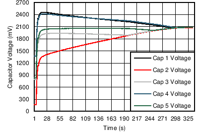
 Figure 19. Voltage Convergence During Capacitor Balancing
