ZHCSEV6A February 2016 – March 2016
PRODUCTION DATA.
- 1 特性
- 2 应用
- 3 说明
- 4 修订历史记录
- 5 Device Comparison Table
- 6 Pin Configuration and Functions
-
7 Specifications
- 7.1 Absolute Maximum Ratings
- 7.2 ESD Ratings
- 7.3 Recommended Operating Conditions
- 7.4 Thermal Information
- 7.5 Supply Current
- 7.6 Digital Input and Output DC Characteristics
- 7.7 Power-On Reset
- 7.8 2.5-V LDO Regulator
- 7.9 Internal Clock Oscillators
- 7.10 ADC (Temperature and Cell Measurement) Characteristics
- 7.11 Integrating ADC (Coulomb Counter) Characteristics
- 7.12 Data Flash Memory Characteristics
- 7.13 I2C-Compatible Interface Communication Timing Characteristics
- 7.14 SDQ Switching Characteristics
- 7.15 Typical Characteristics
- 8 Detailed Description
- 9 Application and Implementation
- 10Power Supply Recommendations
- 11Layout
- 12器件和文档支持
- 13机械、封装和可订购信息
9 Application and Implementation
NOTE
Information in the following applications sections is not part of the TI component specification, and TI does not warrant its accuracy or completeness. TI’s customers are responsible for determining suitability of components for their purposes. Customers should validate and test their design implementation to confirm system functionality.
9.1 Application Information
The bq27320 system-side Li-Ion battery fuel gauge is a microcontroller peripheral that provides fuel gauging for single-cell Li-Ion battery packs. The device requires little system microcontroller firmware development.
The fuel resides on the main board of the system and manages an embedded battery (non-removable) or removable battery pack. To allow for optimal performance in the end application, special considerations must be taken to ensure minimization of measurement error through proper printed circuit board (PCB) board layout.
9.2 Typical Applications
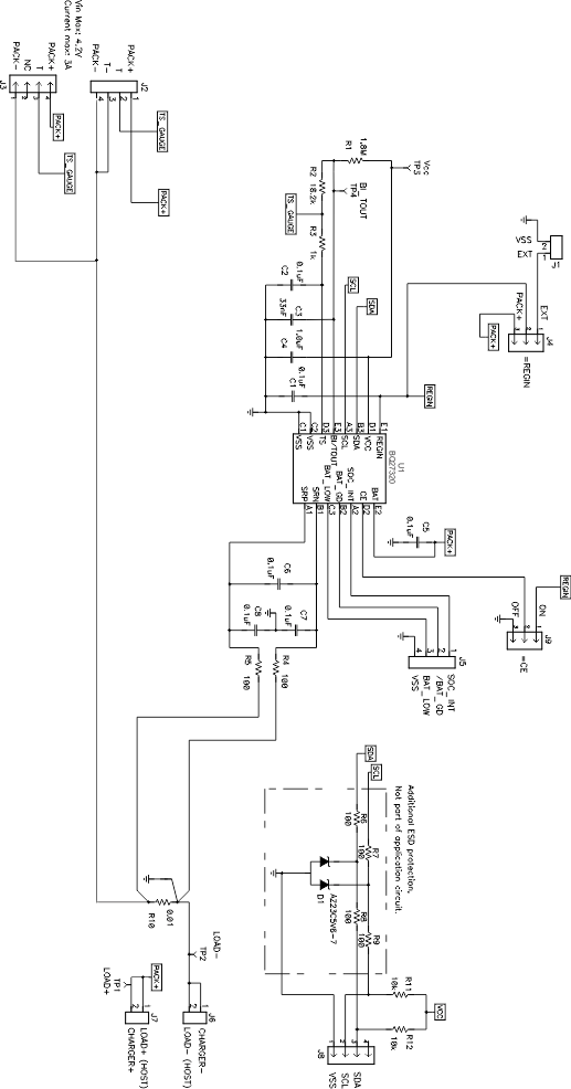 Figure 11. Schematic
9.2.1 Design Requirements
Several key parameters must be updated to align with a given application's battery characteristics. For highest accuracy gauging, it is important to follow-up this initial configuration with a learning cycle to optimize resistance and maximum chemical capacity (Qmax) values prior to sealing and shipping systems to the field. Successful and accurate configuration of the fuel gauge for a target application can be used as the basis for creating a "golden" gas gauge (.fs) file that can be written to all gauges, assuming identical pack design and Li-ion cell origin (chemistry, lot, and so on). Calibration data is included as part of this golden GG file to cut down on system production time. If going this route, it is recommended to average the voltage and current measurement calibration data from a large sample size and use these in the golden file. Table 3, Key Data Flash Parameters for Configuration, shows the items that should be configured to achieve reliable protection and accurate gauging with minimal initial configuration.
Table 3. Key Data Flash Parameters for Configuration
| NAME | DEFAULT | UNIT | RECOMMENDED SETTING |
|---|---|---|---|
| Design Capacity | 1000 | mAh | Set based on the nominal pack capacity as interpreted from cell manufacturer's datasheet. If multiple parallel cells are used, should be set to N × Cell Capacity. |
| Design Energy Scale | 1 | — | Set to 10 to convert all power values to cWh or to 1 for mWh. Design Energy is divided by this value. |
| Reserve Capacity-mAh | 0 | mAh | Set to desired runtime remaining (in seconds / 3600) × typical applied load between reporting 0% SOC and reaching Terminate Voltage, if needed. |
| Chem ID | 0100 | hex | Should be configured using TI-supplied Battery Management Studio software. Default open-circuit voltage and resistance tables are also updated in conjunction with this step. Do not attempt to manually update reported Device Chemistry as this does not change all chemistry information! Always update chemistry using the appropriate software tool (that is, bqStudio). |
| Load Mode | 1 | — | Set to applicable load model, 0 for constant current or 1 for constant power. |
| Load Select | 1 | — | Set to load profile which most closely matches typical system load. |
| Qmax Cell 0 | 1000 | mAh | Set to initial configured value for Design Capacity. The gauge will update this parameter automatically after the optimization cycle and for every regular Qmax update thereafter. |
| Cell0 V at Chg Term | 4200 | mV | Set to nominal cell voltage for a fully charged cell. The gauge will update this parameter automatically each time full charge termination is detected. |
| Terminate Voltage | 3200 | mV | Set to empty point reference of battery based on system needs. Typical is between 3000 and 3200 mV. |
| Ra Max Delta | 44 | mΩ | Set to 15% of Cell0 R_a 4 resistance after an optimization cycle is completed. |
| Charging Voltage | 4200 | mV | Set based on nominal charge voltage for the battery in normal conditions (25°C, etc). Used as the reference point for offsetting by Taper Voltage for full charge termination detection. |
| Taper Current | 100 | mA | Set to the nominal taper current of the charger + taper current tolerance to ensure that the gauge will reliably detect charge termination. |
| Taper Voltage | 100 | mV | Sets the voltage window for qualifying full charge termination. Can be set tighter to avoid or wider to ensure possibility of reporting 100% SOC in outer JEITA temperature ranges that use derated charging voltage. |
| Dsg Current Threshold | 60 | mA | Sets threshold for gauge detecting battery discharge. Should be set lower than minimal system load expected in the application and higher than Quit Current. |
| Chg Current Threshold | 75 | mA | Sets the threshold for detecting battery charge. Can be set higher or lower depending on typical trickle charge current used. Also should be set higher than Quit Current. |
| Quit Current | 40 | mA | Sets threshold for gauge detecting battery relaxation. Can be set higher or lower depending on typical standby current and exhibited in the end system. |
| Avg I Last Run | –299 | mA | Current profile used in capacity simulations at onset of discharge or at all times if Load Select = 0. Should be set to nominal system load. Is automatically updated by the gauge every cycle. |
| Avg P Last Run | –1131 | mW | Power profile used in capacity simulations at onset of discharge or at all times if Load Select = 0. Should be set to nominal system power. Is automatically updated by the gauge every cycle. |
| Sleep Current | 15 | mA | Sets the threshold at which the fuel gauge enters SLEEP mode. Take care in setting above typical standby currents else entry to SLEEP may be unintentionally blocked. |
| CC Gain | 10 | mΩ | Calibrate this parameter using TI-supplied bqStudio software and calibration procedure in the TRM. Determines conversion of coulomb counter measured sense resistor voltage to current. |
| CC Delta | 10 | mΩ | Calibrate this parameter using TI-supplied bqStudio software and calibration procedure in the TRM. Determines conversion of coulomb counter measured sense resistor voltage to passed charge. |
| CC Offset | –1418 | Counts | Calibrate this parameter using TI-supplied bqStudio software and calibration procedure in the TRM. Determines native offset of coulomb counter hardware that should be removed from conversions. |
| Board Offset | 0 | Counts | Calibrate this parameter using TI-supplied bqStudio software and calibration procedure in the TRM. Determines native offset of the printed circuit board parasitics that should be removed from conversions. |
| Pack V Offset | 0 | mV | Calibrate this parameter using TI-supplied bqStudio software and calibration procedure in the TRM. Determines voltage offset between cell tab and ADC input node to incorporate back into or remove from measurement, depending on polarity. |
9.2.2 Detailed Design Procedure
9.2.2.1 BAT Voltage Sense Input
A ceramic capacitor at the input to the BAT pin is used to bypass AC voltage ripple to ground, greatly reducing its influence on battery voltage measurements. It proves most effective in applications with load profiles that exhibit high-frequency current pulses (that is, cell phones) but is recommended for use in all applications to reduce noise on this sensitive high-impedance measurement node.
9.2.2.2 SRP and SRN Current Sense Inputs
The filter network at the input to the coulomb counter is intended to improve differential mode rejection of voltage measured across the sense resistor. These components should be placed as close as possible to the coulomb counter inputs and the routing of the differential traces length-matched to best minimize impedance mismatch-induced measurement errors.
9.2.2.3 Sense Resistor Selection
Any variation encountered in the resistance present between the SRP and SRN pins of the fuel gauge will affect the resulting differential voltage, and derived current, it senses. As such, it is recommended to select a sense resistor with minimal tolerance and temperature coefficient of resistance (TCR) characteristics. The standard recommendation based on best compromise between performance and price is a 1% tolerance, 100-ppm drift sense resistor with a 1-W power rating.
9.2.2.4 TS Temperature Sense Input
Similar to the BAT pin, a ceramic decoupling capacitor for the TS pin is used to bypass AC voltage ripple away from the high-impedance ADC input, minimizing measurement error. Another helpful advantage is that the capacitor provides additional ESD protection since the TS input to system may be accessible in systems that use removable battery packs. It should be placed as close as possible to the respective input pin for optimal filtering performance.
9.2.2.5 Thermistor Selection
The fuel gauge temperature sensing circuitry is designed to work with a negative temperature coefficient-type (NTC) thermistor with a characteristic 10-kΩ resistance at room temperature (25°C). The default curve-fitting coefficients configured in the fuel gauge specifically assume a 103AT-2 type thermistor profile and so that is the default recommendation for thermistor selection purposes. Moving to a separate thermistor resistance profile (for example, JT-2 or others) requires an update to the default thermistor coefficients in data flash to ensure highest accuracy temperature measurement performance.
9.2.2.6 REGIN Power Supply Input Filtering
A ceramic capacitor is placed at the input to the fuel gauge internal LDO to increase power supply rejection (PSR) and improve effective line regulation. It ensures that voltage ripple is rejected to ground instead of coupling into the internal supply rails of the fuel gauge.
9.2.2.7 VCC LDO Output Filtering
A ceramic capacitor is also needed at the output of the internal LDO to provide a current reservoir for fuel gauge load peaks during high peripheral utilization. It acts to stabilize the regulator output and reduce core voltage ripple inside of the fuel gauge.
9.2.3 Application Curves
