ZHCSNY0B May 2020 – January 2023 BQ25798
PRODUCTION DATA
- 1 特性
- 2 应用
- 3 说明
- 4 Revision History
- 5 说明(续)
- 6 Device Comparison
- 7 Pin Configuration and Functions
- 8 Specifications
-
9 Detailed Description
- 9.1 Overview
- 9.2 Functional Block Diagram
- 9.3
Feature Description
- 9.3.1 Device Power-On-Reset
- 9.3.2 PROG Pin Configuration
- 9.3.3 Device Power Up from Battery without Input Source
- 9.3.4 Device Power Up from Input Source
- 9.3.5 Dual-Input Power Mux
- 9.3.6 Buck-Boost Converter Operation
- 9.3.7 USB On-The-Go (OTG)
- 9.3.8 Power Path Management
- 9.3.9 Battery Charging Management
- 9.3.10 Integrated 16-Bit ADC for Monitoring
- 9.3.11 Status Outputs ( STAT, and INT)
- 9.3.12 Ship FET Control
- 9.3.13
Protections
- 9.3.13.1
Voltage and Current Monitoring
- 9.3.13.1.1 VAC Over-voltage Protection (VAC_OVP)
- 9.3.13.1.2 VBUS Over-voltage Protection (VBUS_OVP)
- 9.3.13.1.3 VBUS Under-voltage Protection (POORSRC)
- 9.3.13.1.4 System Over-voltage Protection (VSYS_OVP)
- 9.3.13.1.5 System Short Protection (VSYS_SHORT)
- 9.3.13.1.6 Battery Over-voltage Protection (VBAT_OVP)
- 9.3.13.1.7 Battery Over-current Protection (IBAT_OCP)
- 9.3.13.1.8 Input Over-current Protection (IBUS_OCP)
- 9.3.13.1.9 OTG Over-voltage Protection (OTG_OVP)
- 9.3.13.1.10 OTG Under-voltage Protection (OTG_UVP)
- 9.3.13.2 Thermal Regulation and Thermal Shutdown
- 9.3.13.1
Voltage and Current Monitoring
- 9.3.14 Serial Interface
- 9.4 Device Functional Modes
- 9.5 Register Map
- 10Application and Implementation
- 11Power Supply Recommendations
- 12Layout
- 13Device and Documentation Support
- 14Mechanical, Packaging, and Orderable Information
9.3.5.4 Two ACFETs-RBFETs
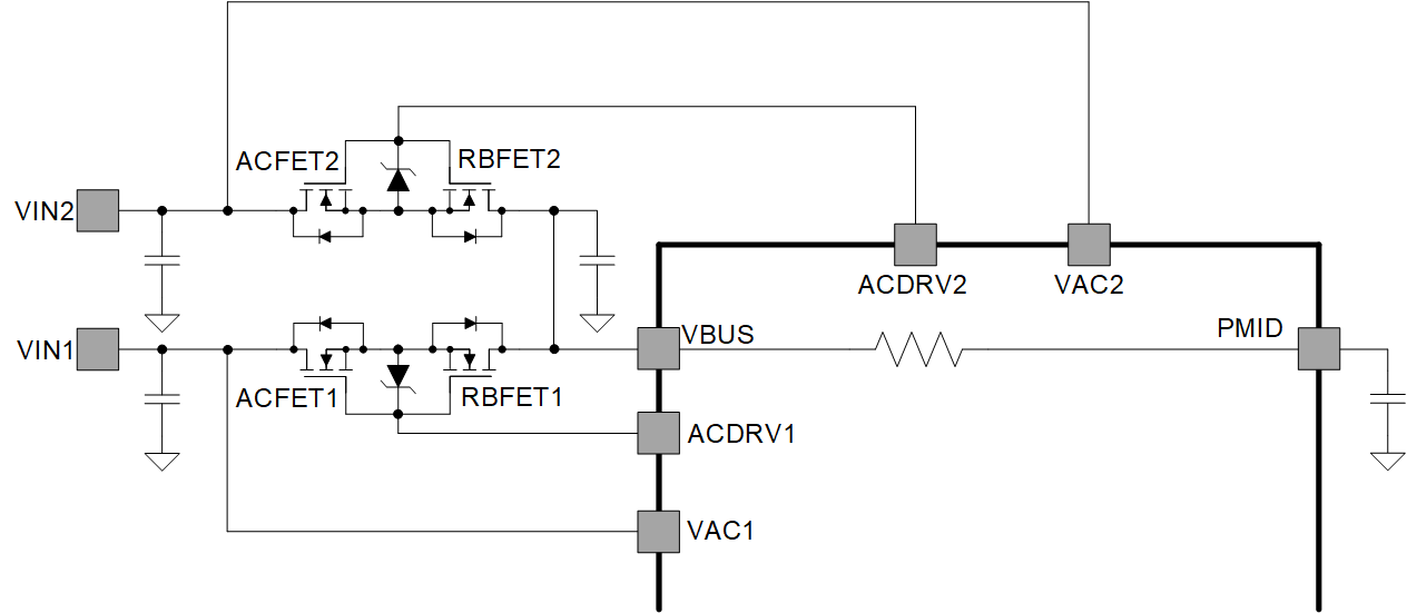
In this scenario, both ACFET1-RBFET1 and ACFET2-RBFET2 are present. VAC1 / VAC2 is tied to the drain of ACFET1 / ACFET2, ACDRV1 / ACDRV2 is connected to the gate of ACFET1 / ACFET2. This structure is developed to support dual-input connected at VAC1 and VAC2. At POR, the charger detects both ACFET1-RBFET1 and ACFET2-RBFET2 present, then updates ACRB1_STAT and ACRB2_STAT to 1.
 Figure 9-4 Two ACFETs-RBFETs Structure
Supporting One Input at VAC1 and One Input at VAC2
Figure 9-4 Two ACFETs-RBFETs Structure
Supporting One Input at VAC1 and One Input at VAC2| PIN OR REGISTER FIELD | STATE |
|---|---|
| External MOSFETs | ACFET1, RBFET1, ACFET2, RBFET2 |
| VAC1 pin | Connected to input source 1 |
| VAC2 pin | Connected to input source 2 |
| ACDRV1 pin | Connected to ACFET1/RBFET1 gate terminals |
| ACDRV2 pin | Connected to ACFET2/RBFET2 gate terminals |
| ACRB1_STAT |
0: ACFET1/RBFET1 Open (Path Disabled)
1: ACFET1/RBFET1 Closed (Path Enabled)
|
| ACRB2_STAT |
0: ACFET2/RBFET2 Open (Path Disabled)
1: ACFET2/RBFET2 Closed (Path Enabled)
|
| DIS_ACDRV |
0: Allow ACDRV1 or ACDRV2 on if all requirements met
1: Force ACDRV1 and ACDRV2 off
|
| EN_ACDRV1 |
0: Force ACDRV1 Off
1: Turn ACDRV1 On if all requirements met
|
| EN_ACDRV2 |
0: Force ACDRV2 Off
1: Turn ACDRV2 On if all requirements met
|
In dual input mode, the ACDRV automatically turns on the ACFET-RBFET of the path where a valid input is first presented, without host intervention.If the two inputs are presented at VAC1 and VAC2 exactly at the same time, ACFET1-RBFET1 with higher priority (port #1 is primary) is turned on while ACFET2-RBFET2 stays off (port #2 is secondary). EN_ACDRV1 is automatically set to 1. If a valid input is presented on the second path while the first path is already on with a valid input, the ACFET-RBFET of the second path remains off. If desired, the host may manually perform a switch between power paths by switching the values of EN_ACDRV1 and EN_ACDRV2. Both EN_ACDRV bits may be updated in a single I2C write operation to minimize the transition time. Note that programming EN_ACDRV1 = 1, EN_ACDRV2 = 1 at the same time to turn on both ACFET1-RBFET1 and ACFET2-RBFET2 is not allowed, and will be ignored by the charger.
To transition from one input to the other, the device first turns off the initially active ACFET-RBFET pair, waits until the VBUS voltage drops lower than VBUS_PRESENT, and then enables the new ACFET-RBFET pair. During this change over, the converter stops switching for a short period of time.
If two valid voltages are present at VAC1 and VAC2 and the source on the connected path becomes invalid because of VAC_UVLO, VAC_OV or IBUS_OC, the charger automatically swaps the input without any host engagement. Any time that the converter autonomously swaps the source paths, it will also update the EN_ACDRV1 and EN_ACDRV2 bits accordingly in order to indicate the active power path.
With only one valid input presented at either VAC1 or VAC2, the ACFET1-RBFET1 and ACFET2-RBFET2 can not be both turned off by setting REG0x13[7:6] = 00. Instead, the host should set DIS_ACDRV = 1 to force both ACFET-RBFET pairs off. With input sources present at both VAC1 and VAC2, the host can turn off the two ACFET-RBFET pairs by setting either REG0x13[7:6] = 00 or DIS_ACDRV = 1.