ZHCSO21 may 2021 BQ25720
PRODUCTION DATA
- 1
- 1 特性
- 2 应用
- 3 说明
- 4 Revision History
- 5 Description (continued)
- 6 Device Comparison Table
- 7 Pin Configuration and Functions
- 8 Specifications
-
9 Detailed Description
- 9.1 Overview
- 9.2 Functional Block Diagram
- 9.3
Feature Description
- 9.3.1 Power-Up Sequence
- 9.3.2 Vmin Active Protection (VAP) with Battery only
- 9.3.3 Two-Level Battery Discharge Current Limit
- 9.3.4 Fast Role Swap Feature
- 9.3.5 CHRG_OK Indicator
- 9.3.6 Input and Charge Current Sensing
- 9.3.7 Input Voltage and Current Limit Setup
- 9.3.8 Battery Cell Configuration
- 9.3.9 Device HIZ State
- 9.3.10 USB On-The-Go (OTG)
- 9.3.11 Converter Operation
- 9.3.12 Inductance Detection Through IADPT Pin
- 9.3.13 Converter Compensation
- 9.3.14 Continuous Conduction Mode (CCM)
- 9.3.15 Pulse Frequency Modulation (PFM)
- 9.3.16 Switching Frequency and Dithering Feature
- 9.3.17 Current and Power Monitor
- 9.3.18 Input Source Dynamic Power Management
- 9.3.19 Input Current Optimizer (ICO)
- 9.3.20 Two-Level Adapter Current Limit (Peak Power Mode)
- 9.3.21 Processor Hot Indication
- 9.3.22
Device Protection
- 9.3.22.1 Watchdog Timer
- 9.3.22.2 Input Overvoltage Protection (ACOV)
- 9.3.22.3 Input Overcurrent Protection (ACOC)
- 9.3.22.4 System Overvoltage Protection (SYSOVP)
- 9.3.22.5 Battery Overvoltage Protection (BATOVP)
- 9.3.22.6 Battery Discharge Overcurrent Protection (BATOC)
- 9.3.22.7 Battery Short Protection (BATSP)
- 9.3.22.8 System Undervoltage Lockout (VSYS_UVP) and Hiccup Mode
- 9.3.22.9 Thermal Shutdown (TSHUT)
- 9.4 Device Functional Modes
- 9.5 Programming
- 9.6
Register Map
- 9.6.1 ChargeOption0 Register (SMBus address = 12h) [reset = E70Eh]
- 9.6.2 ChargeCurrent Register (SMBus address = 14h) [reset = 0000h]
- 9.6.3 ChargeVoltage Register (SMBus address = 15h) [reset value based on CELL_BATPRESZ pin setting]
- 9.6.4 ChargerStatus Register (SMBus address = 20h) [reset = 0000h]
- 9.6.5 ProchotStatus Register (SMBus address = 21h) [reset = B800h]
- 9.6.6 IIN_DPM Register With 10-mΩ Sense Resistor (SMBus address = 22h) [reset = 4100h]
- 9.6.7 ADCVBUS/PSYS Register (SMBus address = 23h)
- 9.6.8 ADCIBAT Register (SMBus address = 24h)
- 9.6.9 ADCIINCMPIN Register (SMBus address = 25h)
- 9.6.10 ADCVSYSVBAT Register (SMBus address = 26h)
- 9.6.11 ChargeOption1 Register (SMBus address = 30h) [reset = 3300h]
- 9.6.12 ChargeOption2 Register (SMBus address = 31h) [reset = 00B7]
- 9.6.13 ChargeOption3 Register (SMBus address = 32h) [reset = 0434h]
- 9.6.14 ProchotOption0 Register (SMBus address = 33h) [reset = 4A81h(2S~) 4A09(1S)]
- 9.6.15 ProchotOption1 Register (SMBus address = 34h) [reset = 41A0h]
- 9.6.16 ADCOption Register (SMBus address = 35h) [reset = 2000h]
- 9.6.17 ChargeOption4 Register (SMBus address = 36h) [reset = 0048h]
- 9.6.18 Vmin Active Protection Register (SMBus address = 37h) [reset = 006Ch(2s~4s)/0004h(1s)]
- 9.6.19 OTGVoltage Register (SMBus address = 3Bh) [reset = 09C4h]
- 9.6.20 OTGCurrent Register (SMBus address = 3Ch) [reset = 3C00h]
- 9.6.21 InputVoltage (VINDPM) Register (SMBus address = 3Dh) [reset = VBUS-1.28V]
- 9.6.22 VSYS_MIN Register (SMBus address = 3Eh) [reset value based on CELL_BATPRESZ pin setting]
- 9.6.23 IIN_HOST Register (SMBus address = 3Fh) [reset = 4100h]
- 9.6.24 ID Registers
- 10Application and Implementation
- 11Power Supply Recommendations
- 12Layout
- 13Device and Documentation Support
- 14Mechanical, Packaging, and Orderable Information
10.2.2.5 Power MOSFETs Selection
Four external N-channel MOSFETs are used for a synchronous switching battery charger. The gate drivers are integrated into the IC with 6 V of gate drive voltage. 30 V or higher voltage rating MOSFETs are preferred for 19-V to 20-V input voltage.
Figure-of-merit (FOM) is usually used for selecting proper MOSFET based on a tradeoff between the conduction loss and switching loss. For the top side MOSFET, FOM is defined as the product of a MOSFET's on-resistance, RDS(ON), and the gate-to-drain charge, QGD. For the bottom side MOSFET, FOM is defined as the product of the MOSFET's on-resistance, RDS(ON), and the total gate charge, QG.
The lower the FOM value, the lower the total power loss. Usually lower RDS(ON) has higher cost with the same package size.
The top-side MOSFET loss includes conduction loss and switching loss. Taking buck mode operation as an example the power loss is a function of duty cycle (D=VOUT/VIN), charging current (ICHG), MOSFET's on-resistance (RDS(ON)_top), input voltage (VIN), switching frequency (fS), turn-on time (ton) and turn-off time (toff):
- IL_DC is the average inductor DC current under buck mode;
- Iripple is the inductor current ripple peak-to-peak value;
The first item Pcon_top represents the conduction loss which is straight forward. The second term Psw_top represents the multiple switching loss items in top MOSFET including voltage and current overlap losses (PIV_top), MOSFET parasitic output capacitance loss (PQoss_top) and gate drive loss (PGate_top). To calculate voltage and current overlap losses (PIV_top):
- ton is the MOSFET turn-on time that VDS falling time from VIN to almost zero (MOSFET turn on conduction voltage);
- toff is the MOSFET turn-off time that IDS falling time from Ipeak to zero;
The MOSFET turn-on and turn-off times are given by:
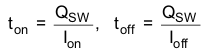
where Qsw is the switching charge, Ion is the turn-on gate driving current, and Ioff is the turn-off gate driving current. If the switching charge is not given in MOSFET datasheet, it can be estimated by gate-to-drain charge (QGD) and gate-to-source charge (QGS):
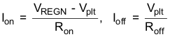
Gate driving current can be estimated by REGN voltage (VREGN), MOSFET plateau voltage (Vplt), total turn-on gate resistance (Ron), and turn-off gate resistance (Roff) of the gate driver:
To calculate top MOSFET parasitic output capacitance loss (PQoss_top):
- Qoss is the MOSFET parasitic output charge which can be found in MOSFET datasheet;
To calculate top MOSFET gate drive loss (PGate_top):
- QGate_top is the top MOSFET gate charge which can be found in MOSFET datasheet;
- Note here VIN is used instead of real gate drive voltage 6 V because, the gate drive 6 V is generated based on LDO from VIN under buck mode, the total gate drive related loss are all considered when VIN is used for gate drive loss calculation .
The bottom-side MOSFET loss also includes conduction loss and switching loss:
The first item Pcon_bottom represents the conduction loss which is straight forward. The second term Psw_bottom represents the multiple switching loss items in bottom MOSFET including reverse recovery losses (PRR_bottom), Dead time body diode conduction loss (PDead_bottom) and gate drive loss (PGate_bottom). The detail calculation can be found below:
- Qrr is the bottom MOSFET reverse recovery charge which can be found in MOSFET data sheet;
- VF is the body diode forward conduction voltage drop;
- tdead_rise is the SW rising edge deadtime between top and bottom MOSFETs which is around 40 ns;
- tdead_fall is the SW falling edge deadtime between top and bottom MOSFETs which is around 30 ns;
PGate_bottom can follow the same method as top MOSFET gate drive loss calculation approach refer to Equation 17.
P-channel MOSFETs is used for battery charging BATFET. The gate drivers are internally integrated into the IC with 10 V of gate drive voltage. 20 V or higher voltage rating MOSFETs are preferred for 1- to 4-cell battery application, the Ciss of P-channel MOSFET should be chosen less than 5 nF.