ZHCSRG2G May 2001 – December 2022 BQ2057C
PRODUCTION DATA
- 1 特性
- 2 应用
- 3 说明
- 4 Revision History
- 5 说明(续)
- 6 Device Comparison Table
- 7 Pin Configuration and Functions
- 8 Specifications
- 9 Detailed Description
-
10Application and Implementation
- 10.1
Application Information
- 10.1.1 Functional Description
- 10.1.2 Qualification and Precharge
- 10.1.3 Current Regulation Phase
- 10.1.4 Voltage Regulation Phase
- 10.1.5 Charge Termination and Recharge
- 10.1.6 Battery Temperature Monitoring
- 10.1.7 Charge Inhibit Function
- 10.1.8 Charge Status Indication
- 10.1.9 Low-power Sleep Mode
- 10.1.10 Selecting an External Pass-Transistor
- 10.1.11 Selecting Input Capacitor
- 10.1.12 Selecting Output Capacitor
- 10.1.13 Automatic Charge-rate Compensation
- 10.2 Typical Application
- 10.1
Application Information
- 11Power Supply Recommendations
- 12Layout
- 13Device and Documentation Support
- 14Mechanical, Packaging, and Orderable Information
封装选项
请参考 PDF 数据表获取器件具体的封装图。
机械数据 (封装 | 引脚)
- D|8
- DGK|8
- PW|8
散热焊盘机械数据 (封装 | 引脚)
订购信息
10.1.4 Voltage Regulation Phase
The voltage regulation feedback is through the BAT pin. This input is tied directly to the positive side of the battery pack. The BQ2057 monitors the battery-pack voltage between the BAT and VSS pins. The BQ2057 is offered in four fixed-voltage versions: 4.1 V, 4.2 V, 8.2 V, and 8.4 V.
Other regulation voltages can be achieved by adding a voltage divider between the positive and negative terminals of the battery pack and using BQ2057T or BQ2057W. The voltage divider presents scaled battery-pack voltage to BAT input. (See Figure 10-7 and Figure 10-8.) The resistor values RB1 and RB2 for the voltage divider are calculated by the following equation:
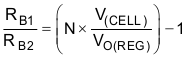
Where:
N = Number of cells in series
V(CELL) = Desired regulation voltage per cell
") Figure 10-7 Optional Voltage Divider for Nonstandard
Regulation Voltage, (High-Side Current
Sensing)
Figure 10-7 Optional Voltage Divider for Nonstandard
Regulation Voltage, (High-Side Current
Sensing)") Figure 10-8 Optional Voltage Divider for Nonstandard
Regulation Voltage, (Low-Side Current
Sensing)
Figure 10-8 Optional Voltage Divider for Nonstandard
Regulation Voltage, (Low-Side Current
Sensing)