ZHCSCR1B July 2014 – August 2014 ADS8684 , ADS8688
PRODUCTION DATA.
- 1 特性
- 2 应用
- 3 说明
- 4 修订历史记录
- 5 Device Comparison Table
- 6 Pin Configuration and Functions
- 7 Specifications
-
8 Detailed Description
- 8.1 Overview
- 8.2 Functional Block Diagram
- 8.3 Feature Description
- 8.4
Device Functional Modes
- 8.4.1 Device Interface
- 8.4.2
Device Modes
- 8.4.2.1 Continued Operation in the Selected Mode (NO_OP)
- 8.4.2.2 Frame Abort Condition (FRAME_ABORT)
- 8.4.2.3 STANDBY Mode (STDBY)
- 8.4.2.4 Power-Down Mode (PWR_DN)
- 8.4.2.5 Auto Channel Enable with Reset (AUTO_RST)
- 8.4.2.6 Manual Channel n Select (MAN_Ch_n)
- 8.4.2.7 Channel Sequencing Modes
- 8.4.2.8 Reset Program Registers (RST)
- 8.5
Register Map
- 8.5.1 Command Register Description
- 8.5.2
Program Register Description
- 8.5.2.1 Program Register Read/Write Operation
- 8.5.2.2 Program Register Map
- 8.5.2.3 Auto-Scan Sequencing Control Registers
- 8.5.2.4 Device Features Selection Control Register (address = 03h)
- 8.5.2.5 Range Select Registers (address = 05h (channel 0), 06h (channel 1), 07h (channel 2), 08h (channel 3), 09h (channel 4), 0Ah (channel 5), 0Bh (channel 6), 0Ch (channel 7))
- 8.5.3 Command Read-Back Register (address = 3Fh)
- 9 Application and Implementation
- 10Power-Supply Recommendations
- 11Layout
- 12器件和文档支持
- 13机械封装和可订购信息
8 Detailed Description
8.1 Overview
The ADS8684 and ADS8688 are 16-bit data acquisition systems with 4- and 8-channel analog inputs, respectively. Each analog input channel consists of an overvoltage protection clamp circuit, a programmable gain amplifier (PGA), and a second-order, antialiasing filter that conditions the input signal before being fed into a 4- or 8-channel analog multiplexer (MUX). The output of the MUX is digitized using a 16-bit analog-to-digital converter (ADC), based on the successive approximation register (SAR) architecture. This overall system can achieve a maximum throughput of 500 kSPS, combined across all channels. The devices feature a 4.096-V internal reference with a fast-settling buffer and a simple SPI-compatible serial interface with a daisy-chain (DAISY) feature.
The devices operate from a single 5-V analog supply and can accommodate true bipolar input signals up to
±2.5 × VREF. The devices offer a constant 1-MΩ resistive input impedance irrespective of the sampling frequency or the selected input range. The integration of multichannel precision analog front-end circuits with high input impedance and a precision ADC operating from a single 5-V supply offers a simplified end solution without requiring external high-voltage bipolar supplies and complicated driver circuits.
8.2 Functional Block Diagram
8.3 Feature Description
8.3.1 Analog Inputs
The ADS8684 and ADS8688 have either four or eight analog input channels, respectively, such that the positive inputs AIN_nP (n = 0 to 3 or 7) are the single-ended analog inputs and the negative inputs AIN_nGND are tied to GND. Figure 51 shows the simplified circuit schematic for each analog input channel, including the input overvoltage protection circuit, PGA, low-pass filter (LPF), high-speed ADC driver, and analog multiplexer.
The devices can support multiple unipolar or bipolar, single-ended input voltage ranges based on the configuration of the program registers. As explained in the Range Select Registers section, the input voltage range for each analog channel can be configured to bipolar ±2.5 × VREF, ±1.25 × VREF, and ±0.625 × VREF or unipolar 0 to 2.5 × VREF and 0 to 1.25 × VREF. With the internal or external reference voltage set to 4.096 V, the input ranges of the device can be configured to bipolar ranges of ±10.24 V, ±5.12 V, and ±2.56 V or unipolar ranges of 0 V to 10.24 V and 0 V to 5.12 V. Any of these input ranges can be assigned to any analog input channel of the device. For instance, the ±2.5 × VREF range can be assigned to AIN_1P, the ±1.25 × VREF range can be assigned to AIN_2P, the 0 V to 2.5 × VREF range can be assigned to AIN_3P, and so forth.
The devices sample the voltage difference (AIN_nP – AIN_nGND) between the selected analog input channel and the AIN_nGND pin. The devices allow a ±0.1-V range on the AIN_nGND pin for all analog input channels. This feature is useful in modular systems where the sensor or signal conditioning block is further away from the ADC on the board and when a difference in the ground potential of the sensor or signal conditioner from the ADC ground is possible. In such cases, TI recommends running separate wires from the AIN_nGND pin of the device to the sensor or signal conditioning ground.
8.3.2 Analog Input Impedance
Each analog input channel in the device presents a constant resistive impedance of 1 MΩ. The input impedance is independent of either the ADC sampling frequency, the input signal frequency, or range. The primary advantage of such high-impedance inputs is the ease of driving the ADC inputs without requiring driving amplifiers with low output impedance. Bipolar, high-voltage power supplies are not required in the system because this ADC does not require any high-voltage front-end drivers. In most applications, the signal sources or sensor outputs can be directly connected to the ADC input, which significantly simplifies the design of the signal chain.
In order to maintain the dc accuracy of the system, matching the external source impedance on the AIN_nP input pin with an equivalent resistance on the AIN_nGND pin is recommended. This matching helps to cancel any additional offset error contributed by the external resistance.
8.3.3 Input Overvoltage Protection Circuit
The ADS8684 and ADS8688 feature an internal overvoltage protection circuit on each of the four or eight analog input channels, respectively. Use these protection circuits as a secondary protection scheme to protect the device. TI highly recommends using external protection devices against surges, electrostatic discharge (ESD), and electrical fast transient (EFT) conditions. The conceptual block diagram of the internal overvoltage protection (OVP) circuit is shown in Figure 52.
 Figure 52. Input Overvoltage Protection Circuit Schematic
As shown in Figure 52, the combination of the 1-MΩ input resistors along with the PGA gain-setting resistors (RFB and RDC) limit the current flowing into the input pins. A combination of antiparallel diodes (D1 and D2) are added on each input pin to protect the internal circuitry and set the overvoltage protection limits.
Table 1 explains the various operating conditions for the device when the device is powered on. Table 1 indicates that when the AVDD pin of the device is connected to the proper supply voltage (AVDD = 5 V) or offers a low impedance of < 30 kΩ, the internal overvoltage protection circuit can withstand up to ±20 V on the analog input pins.
Table 1. Input Overvoltage Protection Limits When AVDD = 5 V or Offers a Low Impedance of < 30 kΩ(1)
| INPUT CONDITION (VOVP = ±20 V) | TEST CONDITION | ADC OUTPUT | COMMENTS | |
|---|---|---|---|---|
| |VIN| < |VRANGE| | Within operating range | All input ranges | Valid | Device functions as per data sheet specifications |
| |VRANGE| < |VIN| < |VOVP| | Beyond operating range but within overvoltage range | All input ranges | Saturated | ADC output is saturated, but device is internally protected (not recommended for extended time) |
| |VIN| > |VOVP| | Beyond overvoltage range | All input ranges | Saturated | This usage condition may cause irreversible damage to the device |
The results indicated in Table 1 are based on an assumption that the analog input pins are driven by very low impedance sources (RS is approximately 0). However, if the sources driving the inputs have higher impedance, the current flowing through the protection diodes reduces further, thereby increasing the OVP voltage range. Note that higher source impedance results in gain errors and contributes to overall system noise performance.
Figure 53 shows the voltage versus current response of the internal overvoltage protection circuit when the device is powered on. According to this current-to-voltage (I-V) response, the current flowing into the device input pins is limited by the 1-MΩ input impedance. However, for voltages beyond ±20 V, the internal node voltages surpass the break-down voltage for internal transistors, thus setting the limit for overvoltage protection on the input pins.
The same overvoltage protection circuit also provides protection to the device when the device is not powered on and AVDD is floating with an impedance > 30 kΩ. This condition can arise when the input signals are applied before the ADC is fully powered on. The overvoltage protection limits for this condition are shown in Table 2.
Table 2. Input Overvoltage Protection Limits When AVDD = Floating with Impedance > 30 kΩ(1)
| INPUT CONDITION (VOVP = ±11 V) | TEST CONDITION | ADC OUTPUT | COMMENTS | |
|---|---|---|---|---|
| |VIN| < |VOVP| | Within overvoltage range | All input ranges | Invalid | Device is not functional but is protected internally by the OVP circuit. |
| |VIN| > |VOVP| | Beyond overvoltage range | All input ranges | Invalid | This usage condition may cause irreversible damage to the device. |
Figure 54 shows the voltage versus current response of the internal overvoltage protection circuit when the device is not powered on. According to this I-V response, the current flowing into the device input pins is limited by the 1-MΩ input impedance. However, for voltages beyond ±11 V, the internal node voltages surpass the break-down voltage for internal transistors, thus setting the limit for overvoltage protection on the input pins.
 Figure 53. I-V Curve for an Input OVP Circuit (AVDD = 5 V)
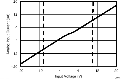 Figure 54. I-V Curve for an Input OVP Circuit
 (AVDD = Floating)
8.3.4 Programmable Gain Amplifier (PGA)
The devices offer a programmable gain amplifier (PGA) at each individual analog input channel, which converts the original single-ended input signal into a fully-differential signal to drive the internal 16-bit ADC. The PGA also adjusts the common-mode level of the input signal before being fed into the ADC to ensure maximum usage of the ADC input dynamic range. Depending on the range of the input signal, the PGA gain can be accordingly adjusted by setting the Range_CHn[2:0] (n = 0 to 3 or 7) bits in the program register. The default or power-on state for the Range_CHn[2:0] bits is 000, which corresponds to an input signal range of ±2.5 × VREF. Table 3 lists the various configurations of the Range_CHn[2:0] bits for the different analog input voltage ranges.
The PGA uses a very highly-matched network of resistors for multiple gain configurations. Matching between these resistors and the amplifiers across all channels is accurately trimmed to keep the overall gain error low across all channels and input ranges.
Table 3. Input Range Selection Bits Configuration
| ANALOG INPUT RANGE | Range_CHn[2:0] | ||
|---|---|---|---|
| BIT 2 | BIT 1 | BIT 0 | |
| ±2.5 × VREF | 0 | 0 | 0 |
| ±1.25 × VREF | 0 | 0 | 1 |
| ±0.625 × VREF | 0 | 1 | 0 |
| 0 to 2.5 × VREF | 1 | 0 | 1 |
| 0 to 1.25 × VREF | 1 | 1 | 0 |
8.3.5 Second-Order, Low-Pass Filter (LPF)
In order to mitigate the noise of the front-end amplifiers and gain resistors of the PGA, each analog input channel of the ADS8684 and ADS8688 features a second-order, antialiasing LPF at the output of the PGA. The magnitude and phase response of the analog antialiasing filter are shown in Figure 55 and Figure 56, respectively. For maximum performance, the –3-dB cutoff frequency for the antialiasing filter is typically set to
15 kHz. The performance of the filter is consistent across all input ranges supported by the ADC.
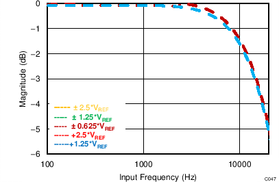 Figure 55. Second-Order LPF Magnitude Response
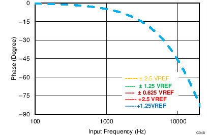 Figure 56. Second-Order LPF Phase Response
8.3.6 ADC Driver
In order to meet the performance of a 16-bit, SAR ADC at the maximum sampling rate (500 kSPS), the sample-and-hold capacitors at the input of the ADC must be successfully charged and discharged during the acquisition time window. This drive requirement at the inputs of the ADC necessitates the use of a high-bandwidth, low-noise, and stable amplifier buffer. Such an input driver is integrated in the front-end signal path of each analog input channel of the device. During transition from one channel of the multiplexer to another channel, the fast integrated driver ensures that the multiplexer output settles to 16-bit accuracy within the acquisition time of the ADC, irrespective of the input levels on the respective channels.
8.3.7 Multiplexer (MUX)
The ADS8684 and ADS8688 feature an integrated 4- and 8-channel analog multiplexer, respectively. For each analog input channel, the voltage difference between the positive analog input AIN_nP and the negative ground input AIN_nGND is conditioned by the analog front-end circuitry before being fed into the multiplexer. The output of the multiplexer is directly sampled by the ADC. The multiplexer in the device can scan these analog inputs in either manual or auto-scan mode, as explained in Channel Sequencing Modes section. In manual mode (MAN_Ch_n), the channel is selected for every sample via a register write; in auto-scan mode (AUTO_RST), the channel number is incremented automatically on every CS falling edge after the present channel is sampled. The analog inputs can be selected for an auto scan with register settings (refer to Auto-Scan Sequencing Control Registers section). The devices automatically scan only the selected analog inputs in ascending order.
The maximum overall throughput for the ADS8684 and ADS8688 is specified at 500 kSPS across all channels. The per channel throughput is dependent on the number of channels selected in the multiplexer scanning sequence. For example, the throughput per channel is equal to 250 kSPS if only two channels are selected, but is equal to 125 kSPS per channel if four channels are selected (as in the ADS8684), and so forth.
Refer to Table 6 for command register settings to switch between the auto-scan mode and manual mode for individual analog channels.
8.3.8 Reference
The ADS8684 and ADS8688 can operate with either an internal voltage reference or an external voltage reference using the internal buffer. The internal or external reference selection is determined by an external REFSEL pin. The devices have a built-in buffer amplifier to drive the actual reference input of the internal ADC core for maximizing performance.
8.3.8.1 Internal Reference
The devices have an internal 4.096-V (nominal value) reference. In order to select the internal reference, the REFSEL pin must be tied low or connected to AGND. When the internal reference is used, REFIO (pin 5) becomes an output pin with the internal reference value. TI recommends placing a 10-µF (minimum) decoupling capacitor between the REFIO pin and REFGND (pin 6), as shown in Figure 57. The capacitor must be placed as close to the REFIO pin as possible. The output impedance of the internal band-gap circuit creates a low-pass filter with this capacitor to band-limit the noise of the reference. The use of a smaller capacitor value allows higher reference noise in the system, thus degrading SNR and SINAD performance. Do not use the REFIO pin to drive external ac or dc loads because REFIO has limited current output capability. The REFIO pin can be used as a source if followed by a suitable op amp buffer (such as the OPA320).
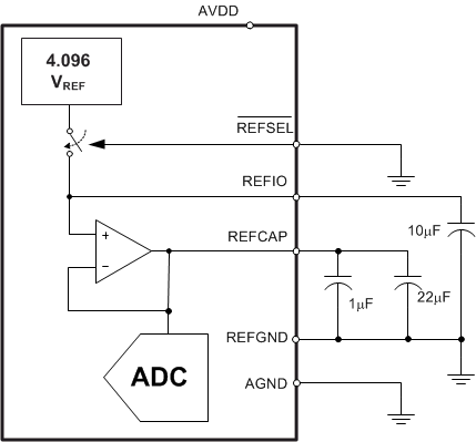 Figure 57. Device Connections for Using an Internal 4.096-V Reference
The device internal reference is factory trimmed to a maximum initial accuracy of ±1 mV. The histogram in Figure 58 shows the distribution of the internal voltage reference output taken from more than 3300 production devices.
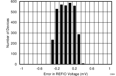 Figure 58. Internal Reference Accuracy at Room Temperature Histogram
The initial accuracy specification for the internal reference can be degraded if the die is exposed to any mechanical or thermal stress. Heating the device while being soldered to a PCB and any subsequent solder reflow is a primary cause for shifts in the VREF value. The main cause of thermal hysteresis is a change in die stress and therefore is a function of the package, die-attach material, and molding compound, as well as the layout of the device itself.
In order to illustrate this effect, 80 devices were soldered using lead-free solder paste with the manufacturer's suggested reflow profile, as explained in the Application Report AN-2029 Handling & Process Recommendations (SNOA550). The internal voltage reference output is measured before and after the reflow process and the typical shift in value is displayed in Figure 59. Although all tested units exhibit a positive shift in their output voltages, negative shifts are also possible. Note that the histogram in Figure 59 displays the typical shift for exposure to a single reflow profile. Exposure to multiple reflows, which is common on PCBs with surface-mount components on both sides, causes additional shifts in the output voltage. If the PCB is to be exposed to multiple reflows, solder the ADS8684 and ADS8688 in the second pass to minimize device exposure to thermal stress.
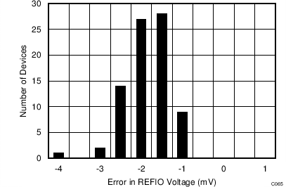 Figure 59. Solder Heat Shift Distribution Histogram
The internal reference is also temperature compensated to provide excellent temperature drift over an extended industrial temperature range of –40°C to 125°C. Figure 60 shows the variation of the internal reference voltage across temperature for different values of the AVDD supply voltage. The typical specified value of the reference voltage drift over temperature is 6 ppm/°C (Figure 61) and the maximum specified temperature drift is equal to
10 ppm/°C.
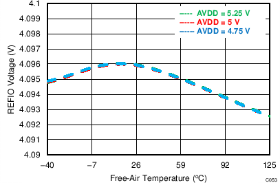
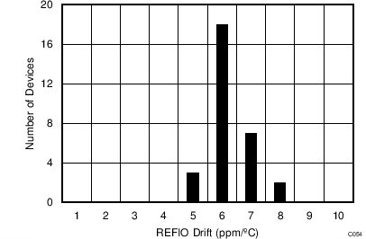
| AVDD = 5 V, Number of Devices = 30, ΔT = –40°C to 125°C |
8.3.8.2 External Reference
For applications that require a better reference voltage or a common reference voltage for multiple devices, the ADS8684 and ADS8688 offer a provision to use an external reference along with an internal buffer to drive the ADC reference pin. In order to select the external reference mode, either tie the REFSEL pin high or connect this pin to the DVDD supply. In this mode, an external 4.096-V reference must be applied at REFIO (pin 5), which becomes an input pin. Any low-power, low-drift, or small-size external reference can be used in this mode because the internal buffer is optimally designed to handle the dynamic loading on the REFCAP pin, which is internally connected to the ADC reference input. The output of the external reference must be appropriately filtered to minimize the resulting effect of the reference noise on system performance. A typical connection diagram for this mode is shown in Figure 62.
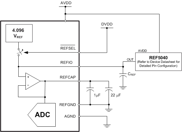 Figure 62. Device Connections for Using an External 4.096-V Reference
The output of the internal reference buffer appears at the REFCAP pin. A minimum capacitance of 10 µF must be placed between REFCAP (pin 7) and REFGND (pin 6). Place another capacitor of 1 µF as close to the REFCAP pin as possible for decoupling high-frequency signals. Do not use the internal buffer to drive external ac or dc loads because of the limited current output capability of this buffer.
The performance of the internal buffer output is very stable across the entire operating temperature range of –40°C to 125°C. Figure 63 shows the variation in the REFCAP output across temperature for different values of the AVDD supply voltage. The typical specified value of the reference buffer drift over temperature is 1 ppm/°C (Figure 64) and the maximum specified temperature drift is equal to 1.5 ppm/°C.
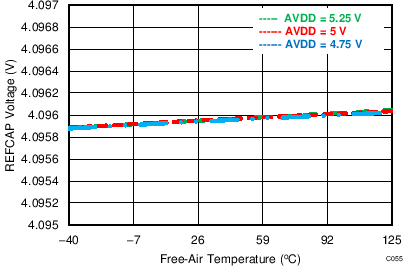
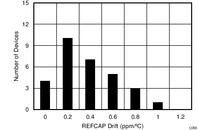
| AVDD = 5 V, Number of Devices = 30, ΔT = –40°C to 125°C |
8.3.9 Auxiliary Channel
The devices include a single-ended auxiliary input channel (AUX_IN and AUX_GND). The AUX channel provides direct interface to an internal, high-precision, 16-bit ADC through the multiplexer because this channel does not include the front-end analog signal conditioning that the other analog input channels have. The AUX channel supports a single unipolar input range of 0 V to VREF because there is no front-end PGA. The input signal on the AUX_IN pin can vary from 0 V to VREF, whereas the AUX_GND pin must be tied to GND.
When a conversion is initiated, the voltage between these pins is sampled directly on an internal sampling capacitor (75 pF, typical). The input current required to charge the sampling capacitor is determined by several factors, including the sampling rate, input frequency, and source impedance. For slow applications that use a low-impedance source, the inputs of the AUX channel can be directly driven. When the throughput, input frequency, or the source impedance increases, a driving amplifier must be used at the input to achieve good ac performance from the AUX channel. Some key requirements of the driving amplifier are discussed in the Input Driver for the AUX Channel section.
The AUX channel in the ADS8684 and ADS8688 offers a true 16-bit performance with no missing codes. Some typical performance characteristics of the AUX channel are illustrated in Figure 65 to Figure 68.
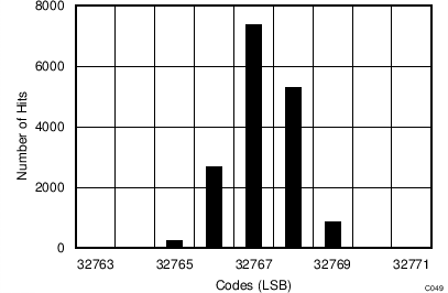
| Mean = 32767.15, Sigma = 0.83, Input = 0.5 × VREF |
(AUX Channel)
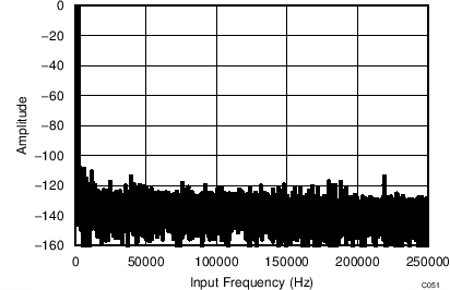
| fIN = 1 kHz, SNR = 88.2 dB, SINAD = 88.1 dB, THD = –102 dB, SFDR = 102 dB, Number of points = 64k |
(AUX Channel)
| AUX Channel |
(AUX Channel)
| fIN = 1 kHz |
(AUX Channel)
8.3.9.1 Input Driver for the AUX Channel
For applications that use the AUX input channels at high throughput and high input frequency, a driving amplifier with low output impedance is required to meet the ac performance of the internal 16-bit ADC. Some key specifications of the input driving amplifier are discussed below:
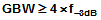
- Small-signal bandwidth. The small-signal bandwidth of the input driving amplifier must be much higher than the bandwidth of the AUX input to ensure that there is no attenuation of the input signal resulting from the bandwidth limitation of the amplifier. In a typical data acquisition system, a low cut-off frequency, antialiasing filter is used at the inputs of a high-resolution ADC. The amplifier driving the antialiasing filter must have a low closed-loop output impedance for stability, which implies a higher gain bandwidth for the amplifier. Higher small-signal bandwidth also minimizes the harmonic distortion at higher input frequencies. In general, the amplifier bandwidth requirements can be calculated on the basis of Equation 1.
- f–3dB is the 3-dB bandwidth of the RC filter.
- Distortion. In order to achieve the distortion performance of the AUX channel, the distortion of the input driver must be at least 10 dB lower than the specified distortion of the internal ADC, as shown in Equation 2.
- Noise. Careful considerations must be made to select a low-noise, front-end amplifier in order to prevent any degradation in SNR performance of the system. As a rule of thumb, to ensure that the noise performance of the data acquisition system is not limited by the front-end circuit, keep the total noise contribution from the front-end circuit below 20% of the input-referred noise of the ADC. Noise from the input driver circuit is band-limited by the low cut-off frequency of the input antialiasing filter, as explained in Equation 3.
- V1 / f_AMP_PP is the peak-to-peak flicker noise,
- en_RMS is the amplifier broadband noise density in nV/√Hz, and
- NG is the noise gain of the front-end circuit, which is equal to 1 in a buffer configuration.
where

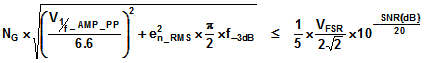
where
8.3.10 ADC Transfer Function
The ADS8684 and ADS8688 are a family of multichannel devices that support single-ended, bipolar, and unipolar input ranges on all input channels. The output of the devices is in straight binary format for both bipolar and unipolar input ranges. The format for the output codes is the same across all analog channels.
The ideal transfer characteristic for each ADC channel for all input ranges is shown in Figure 69. The full-scale range (FSR) for each input signal is equal to the difference between the positive full-scale (PFS) input voltage and the negative full-scale (NFS) input voltage. The LSB size is equal to FSR / 216 = FSR / 65536 because the resolution of the ADC is 16 bits. For a reference voltage of VREF = 4.096 V, the LSB values corresponding to the different input ranges are listed in Table 4.
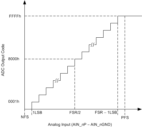 Figure 69. 16-Bit ADC Transfer Function (Straight Binary Format)
Table 4. ADC LSB Values for Different Input Ranges (VREF = 4.096 V)
| INPUT RANGE | POSITIVE FULL SCALE | NEGATIVE FULL SCALE | FULL-SCALE RANGE | LSB (µV) |
|---|---|---|---|---|
| ±2.5 × VREF | 10.24 V | –10.24 V | 20.48 V | 312.50 |
| ±1.25 × VREF | 5.12 V | –5.12 V | 10.24 V | 156.25 |
| ±0.625 × VREF | 2.56 V | –2.56 V | 5.12 V | 78.125 |
| 0 to 2.5 × VREF | 10.24 V | 0 V | 10.24 V | 156.25 |
| 0 to 1.25 × VREF | 5.12 V | 0 V | 5.12 V | 78.125 |
8.4 Device Functional Modes
8.4.1 Device Interface
8.4.1.1 Digital Pin Description
The digital data interface for the ADS8684 and ADS8688 is illustrated in Figure 70.
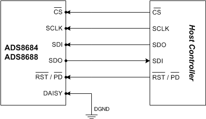 Figure 70. Pin Configuration for the Digital Interface
The signals shown in Figure 70 are summarized as follows:
8.4.1.1.1 CS (Input)
CS indicates an active-low, chip-select signal. CS is also used as a control signal to trigger a conversion on the falling edge. Each data frame begins with the falling edge of the CS signal. The analog input channel to be converted during a particular frame is selected in the previous frame. On the CS falling edge, the devices sample the input signal from the selected channel and a conversion is initiated using the internal clock. The device settings for the next data frame can be input during this conversion process. When the CS signal is high, the ADC is considered to be in an idle state.
8.4.1.1.2 SCLK (Input)
This pin indicates the external clock input for the data interface. All synchronous accesses to the device are timed with respect to the falling edges of the SCLK signal.
8.4.1.1.3 SDI (Input)
SDI is the serial data input line. SDI is used by the host processor to program the internal device registers for device configuration. At the beginning of each data frame, the CS signal goes low and the data on the SDI line are read by the device at every falling edge of the SCLK signal for the next 16 SCLK cycles. Any changes made to the device configuration in a particular data frame are applied to the device on the subsequent falling edge of the CS signal.
8.4.1.1.4 SDO (Output)
SDO is the serial data output line. SDO is used by the device to output conversion data. The size of the data output frame varies depending on the register setting for the SDO format; see Table 13. A low level on CS releases the SDO pin from the Hi-Z state. SDO is kept low for the first 15 SCLK falling edges. The MSB of the output data stream is clocked out on SDO on the 16th SCLK falling edge, followed by the subsequent data bits on every falling edge thereafter. The SDO line goes low after the entire data frame is output and goes to a Hi-Z state when CS goes high.
8.4.1.1.5 DAISY (Input)
DAISY is a serial input pin. When multiple devices are connected in daisy-chain mode, as illustrated in Figure 73, the DAISY pin of the first device in the chain is connected to GND. The DAISY pin of every subsequent device is connected to the SDO output pin of the previous device, and the SDO output of the last device in the chain goes to the SDI of the host processor. If an application uses a stand-alone device, the DAISY pin is connected to GND.
8.4.1.1.6 RST/PD (Input)
RST/PD is a dual-function pin. Figure 71 shows the timing of this pin and Table 5 explains the usage of this pin.
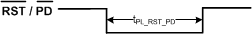 Figure 71. RST/PD Pin Timing
Table 5. RST/PD Pin Functionality
| CONDITION | DEVICE MODE |
|---|---|
| 40 ns < tPL_RST_PD ≤ 100 ns | The device is in RST mode and does not enter PWR_DN mode. |
| 100 ns < tPL_RST_PD < 400 ns | The device is in RST mode and may or may not enter PWR_DN mode. NOTE: This setting is not recommended. |
| tPL_RST_PD ≥ 400 ns | The device enters PWR_DN mode and the program registers are reset to default value. |
The devices can be placed into power-down (PWR_DN) mode by pulling the RST/PD pin to a logic low state for at least 400 ns. The RST/PD pin is asynchronous to the clock; thus, RST/PD can be triggered at any time regardless of the status of other pins (including the analog input channels). When the device is in power-down mode, any activity on the digital input pins (apart from the RST/PD pin) is ignored.
The program registers in the device can be reset to their default values (RST) by pulling the RST/PD pin to a logic low state for no longer than 100 ns. This input is asynchronous to the clock. When RST/PD is pulled back to a logic high state, the devices are placed in normal mode. One valid write operation must be executed on the program register in order to configure the device, followed by an appropriate command (AUTO_RST or MAN) to initiate conversions.
When the RST/PD pin is pulled back to a logic high level, the devices wake-up in a default state in which the program registers are reset to their default values.
8.4.1.2 Data Acquisition Example
This section provides an example of how a host processor can use the device interface to configure the device internal registers as well as convert and acquire data for sampling a particular input channel. The timing diagram shown in Figure 72 provides further details.
 Figure 72. Device Operation Using the Serial Interface Timing Diagram
There are four events shown in Figure 72. These events are described below:
- Event 1: The host initiates a data conversion frame through a falling edge of the CS signal. The analog input signal at the instant of the CS falling edge is sampled by the ADC and conversion is performed using an internal oscillator clock. The analog input channel converted during this frame is selected in the previous data frame. The internal register settings of the device for the next conversion can be input during this data frame using the SDI and SCLK inputs. Initiate SCLK at this instant and latch data on the SDI line into the device on every SCLK falling edge for the next 16 SCLK cycles. At this instant, SDO goes low because the device does not output internal conversion data on the SDO line during the first 16 SCLK cycles.
- Event 2: During the first 16 SCLK cycles, the device completes the internal conversion process and data are now ready within the converter. However, the device does not output data bits on SDO until the 16th falling edge appears on the SCLK input. Because the ADC conversion time is fixed (the maximum value is given in the Electrical Characteristics table), the 16th SCLK falling edge must appear after the internal conversion is over, otherwise data output from the device is incorrect. Therefore, the SCLK frequency cannot exceed a maximum value, as provided in the Timing Requirements: Serial Interface table.
- Event 3: At the 16th falling edge of the SCLK signal, the device reads the LSB of the input word on the SDI line. The device does not read anything from the SDO line for the remaining data frame. On the same edge, the MSB of the conversion data is output on the SDO line and can be read by the host processor on the subsequent falling edge of the SCLK signal. For 16 bits of output data, the LSB can be read on the 32nd SCLK falling edge. The SDO outputs 0 on subsequent SCLK falling edges until the next conversion is initiated.
- Event 4: When the internal data from the device is received, the host terminates the data frame by deactivating the CS signal to high. The SDO output goes into a Hi-Z state until the next data frame is initiated, as explained in Event 1.
8.4.1.3 Host-to-Device Connection Topologies
The digital interface of the ADS8684 and ADS8688 offers a lot of flexibility in the ways that a host controller can exchange data or commands with the device. A typical connection between a host controller and a stand-alone device is illustrated in Figure 70. However, there are applications that require multiple ADCs but the host controller has limited interfacing capability. This section describes two connection topologies that can be used to address the requirements of such applications.
8.4.1.3.1 Daisy-Chain Topology
A typical connection diagram showing multiple devices in daisy-chain mode is shown in Figure 73. The CS, SCLK, and SDI inputs of all devices are connected together and controlled by a single CS, SCLK, and SDO pin of the host controller, respectively. The DAISY1 input pin of the first ADC in the chain is connected to DGND, the SDO1 output pin is connected to the DAISY2 input of ADC2, and so forth. The SDON pin of the Nth ADC in the chain is connected to the SDI pin of the host controller. The devices do not require any special hardware or software configuration to enter daisy-chain mode.
 Figure 73. Daisy-Chain Connection Schematic
A typical timing diagram for three devices connected in daisy-chain mode is shown in Figure 74.
 Figure 74. Three Devices Connected in Daisy-Chain Mode Timing Diagram
At the falling edge of the CS signal, all devices sample the input signal at their respective selected channels and enter into conversion phase. For the first 16 SCLK cycles, the internal register settings for the next conversion can be entered using the SDI line, which is common to all devices in the chain. During this time period, the SDO outputs for all devices remain low. At the end of conversion, every ADC in the chain loads its own conversion result into an internal 16-bit shift register. At the 16th SCLK falling edge, every ADC in the chain outputs the MSB bit on its own SDO output pin. On every subsequent SCLK falling edge, the internal shift register of each ADC latches the data available on its DAISY pin and shifts out the next bit of data on its SDO pin. Therefore, the digital host receives the data of ADCN, followed by the data of ADCN–1, and so forth (in MSB-first fashion). In total, a minimum of 16 × N SCLK falling edges are required to capture the outputs of all N devices in the chain. This example uses three devices in a daisy-chain connection, so 3 × 16 = 48 SCLK cycles are required to capture the outputs of all devices in the chain along with the 16 SCLK cycles to input the register settings for the next conversion, resulting in a total of 64 SCLK cycles for the entire data frame. Note that the overall throughput of the system is proportionally reduced with the number of devices connected in a daisy-chain configuration.
The following points must be noted about the daisy-chain configuration illustrated in Figure 73:
- The SDI pins for all devices are connected together so each device operates with the same internal configuration. This limitation can be overcome by spending additional host controller resources to control the SDI input of devices with unique configurations.
- If the number of devices connected in daisy-chain is more than four, loading increases on the shared output lines from the host controller (CS, SDO, and SCLK). This increased loading may lead to digital timing errors. This limitation can be overcome by using digital buffers on the shared outputs from the host controller before feeding the shared digital lines into additional devices.
8.4.1.3.2 Star Topology
A typical connection diagram showing multiple devices in the star topology is shown in Figure 75. The SDI and SCLK inputs of all devices are connected together and are controlled by a single SDO and SCLK pin of the host controller, respectively. Similarly, the SDO outputs of all devices are tied together and connected to the SDI input pin of the host controller. The CS input pin of each device is individually controlled by separate CS control lines from the host controller.
 Figure 75. Star Topology Connection Schematic
The timing diagram for a typical data frame in the star topology is the same as in a stand-alone device operation, as illustrated in Figure 72. The data frame for a particular device starts with the falling edge of the CS signal and ends when the CS signal goes high. Because the host controller provides separate CS control signals for each device in this topology, the user can select the devices in any order and initiate a conversion by bringing down the CS signal for that particular device. As explained in Figure 72, when CS goes high at the end of each data frame, the SDO output of the device is placed into a Hi-Z state. Therefore, the shared SDO line in the star topology is controlled only by the device with an active data frame (CS is low). In order to avoid any conflict related to multiple devices driving the SDO line at the same time, ensure that the host controller pulls down the CS signal for only one device at any particular time.
TI recommends connecting a maximum of four devices in the star topology. Beyond that, loading may increase on the shared output lines from the host controller (SDO and SCLK). This loading may lead to digital timing errors. This limitation can be overcome by using digital buffers on the shared outputs from the host controller before being fed into additional devices.
8.4.2 Device Modes
The ADS8684 and ADS8688 support multiple modes of operation that are software programmable. After powering up, the device is placed into idle mode and does not perform any function until a command is received from the user. Table 6 lists all commands to enter the different modes of the device. After power-up, the program registers wake up with the default values and require appropriate configuration settings before performing any conversion. The diagram in Figure 76 explains how to switch the device from one mode of operation to another.
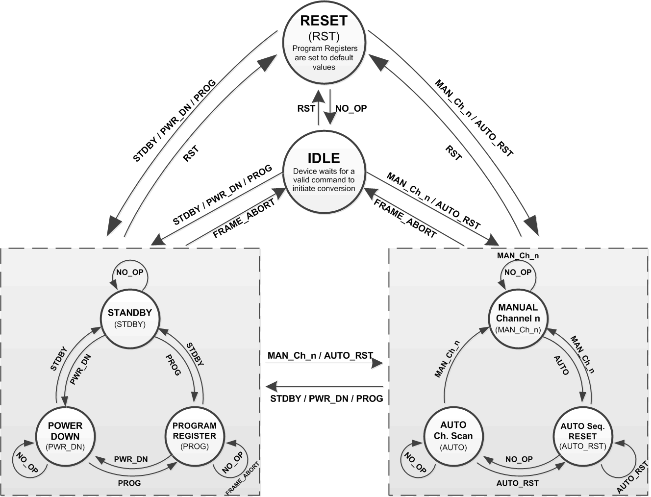 Figure 76. State Transition Diagram
8.4.2.1 Continued Operation in the Selected Mode (NO_OP)
Holding the SDI line low continuously (equivalent to writing a 0 to all 16 bits) during device operation continues device operation in the last selected mode (STDBY, PWR_DN or AUTO_RST, MAN_Ch_n). In this mode, the device follows the same settings that are already configured in the program registers (addresses 01h to 3Ch).
8.4.2.2 Frame Abort Condition (FRAME_ABORT)
As explained in the Data Acquisition Example section, the device digital interface is designed such that each data frame starts with a falling edge of the CS signal. During the first 16 SCLK cycles, the device reads the 16-bit command word on the SDI line. The device waits to execute the command until the last bit of the command is received, which is latched on the 16th SCLK falling edge. During this operation, the CS signal must stay low. If the CS signal goes high for any reason before the data transmission is complete, the device goes into IDLE state and waits for a proper command to be written. This condition is called the FRAME_ABORT condition. When the device is operating in IDLE mode, any read operation on the device returns all 1's on the SDO line.
If a FRAME_ABORT condition occurs when the device is performing any read or write operation in the program register (PROG mode), then the device adopts the previous settings of the program registers until the user executes a proper command to execute the program register read or write command.
8.4.2.3 STANDBY Mode (STDBY)
The devices support a low-power standby mode (STDBY) in which only part of the circuit is powered down. The internal reference and buffer is not powered down, and therefore, the device can be quickly powered up in 20 µs on exiting the STDBY mode. When the device comes out of STDBY mode, the program registers are not reset to the default values.
To enter STDBY mode, execute a valid write operation to the command register with a STDBY command of 8200h, as shown in Figure 77. The command is executed and the device enters STDBY mode on the next CS rising edge following this write operation. The device remains in STDBY mode if no valid conversion command (AUTO_RST or MAN_Ch_n) is executed and SDI remains low (refer to the Continued Operation in the Selected Mode section) during the subsequent data frames. When the device operates in STDBY mode the program register settings can be updated, as explained in Program Register Read/Write Operation section using 16 SCLK cycles. However, if the user provides complete 32 SCLK cycles, then the SDO line yields all 1's on the last 16 SCLK cycles because there is no ongoing conversion in STDBY mode. The program register read operation can take place normally during this mode.
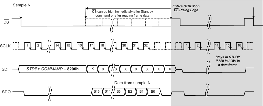 Figure 77. Enter and Remain in STDBY Mode Timing Diagram
In order to exit STDBY mode a valid 16-bit write command must be executed to enter auto (AUTO_RST) or manual (MAN_CH_n) scan mode, as shown in Figure 78. The device starts exiting STDBY mode on the next CS rising edge. At the next CS falling edge, the device samples the analog input at the channel selected by the MAN_CH_n command or the first channel of the AUTO_RST mode sequence. To ensure that the input signal is sampled correctly, keep the minimum width of the CS signal at 20 µs after exiting STDBY mode so the device can be fully powered up before taking the sample. The data output for the selected channel can be read during the same data frame, as explained in Figure 72.
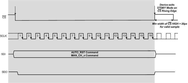 Figure 78. Exit STDBY Mode Timing Diagram
8.4.2.4 Power-Down Mode (PWR_DN)
The devices support a hardware and software power-down mode (PWR_DN) in which all internal circuitry is powered down, including the internal reference and buffer. A minimum time of 15 ms is required for the device to power up and convert the selected analog input channel after exiting PWR_DN mode, if the device is operating in the internal reference mode (REFSEL = 0). The hardware power mode for the device is explained in the RST/PD (Input) section. The primary difference between the hardware and software power-down modes is that the program registers are reset to default values when the devices wake up from hardware power-down, but the previous settings of the program registers are retained when the devices wake up from software power-down.
To enter PWR_DN mode using software, execute a valid write operation on the command register with a software PWR_DN command of 8300h, as shown in Figure 79. The command is executed and the device enters PWR_DN mode on the next CS rising edge following this write operation. The device remains in PWR_DN mode if no valid conversion command (AUTO_RST or MAN_Ch_n) is executed and SDI remains low (refer to the Continued Operation in the Selected Mode section) during the subsequent data frames. When the device operates in PWR_DN mode the program register settings can be updated, as explained in Program Register Read/Write Operation section using 16 SCLK cycles. However, if the user provides complete 32 SCLK cycles, then the SDO line yields all 1's on the last 16 SCLK cycles because there is no ongoing conversion in PWR_DN mode. The program register read operation can take place normally during this mode.
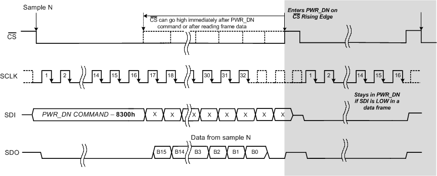 Figure 79. Enter and Remain in PWR_DN Mode Timing Diagram
In order to exit from PWR_DN mode a valid 16-bit write command must be executed, as shown in Figure 80. The device comes out of PWR_DN mode on the next CS rising edge. For operation in internal reference mode (REFSEL = 0), 15 ms are required for the device to power-up the reference and other internal circuits and settle to the required accuracy before valid conversion data are output for the selected input channel.
 Figure 80. Exit PWR_DN Mode Timing Diagram
8.4.2.5 Auto Channel Enable with Reset (AUTO_RST)
The devices can be programmed to scan the input signal on all analog channels automatically by writing a valid auto channel sequence with a reset (AUTO_RST, A000h) command in the command register, as explained in Figure 81. The sequence of channels for the automatic scan can be configured by the AUTO SCAN sequencing control register (01h to 02h) in the program register; refer to the Program Register Map section. In this mode, the devices continuously cycle through the selected channels in ascending order, beginning with the lowest channel and converting all channels selected in the program register. On completion of the sequence, the devices return to the lowest count channel in the program register and repeat the sequence. The input voltage range for each channel in the auto-scan sequence can be configured by setting the Range Select Registers of the program registers.
 Figure 81. Enter AUTO_RST Mode Timing Diagram
The devices remain in AUTO_RST mode if no other valid command is executed and SDI is kept low (refer to the Continued Operation in the Selected Mode (NO_OP) section) during subsequent data frames. If the AUTO_RST command is executed again at any time during this mode of operation, then the sequence of the scanned channels is reset. The devices return to the lowest count channel of the auto-scan sequence in the program register and repeat the sequence. The timing diagram in Figure 82 shows this behavior using an example in which channels 0 to 3 are selected in the auto sequence. For switching between AUTO_RST mode and MAN_Ch_n mode, refer to the Channel Sequencing Modes section.
 Figure 82. Device Operation Example in AUTO_RST Mode
8.4.2.6 Manual Channel n Select (MAN_Ch_n)
The devices can be programmed to convert a particular analog input channel by operating in manual channel n scan mode (MAN_Ch_n). This programming is done by writing a valid manual channel n select command (MAN_Ch_n) in the command register, as shown in Figure 83. Refer to Table 6 for a list of commands to select individual channels during MAN_Ch_n mode.
 Figure 83. Enter MAN_Ch_n Scan Mode Timing Diagram
The manual channel n select command (MAN_Ch_n) is executed and the devices sample the analog input on the selected channel on the CS falling edge of the next data frame following this write operation. The input voltage range for each channel in the MAN_Ch_n mode can be configured by setting the Range Select Registers in the program registers. The device continues to sample the analog input on the same channel if no other valid command is executed and SDI is kept low (refer to the Continued Operation in the Selected Mode (NO_OP) section) during subsequent data frames. The timing diagram in Figure 84 illustrates this behavior using an example in which channel 1 is selected in the manual sequencing mode. For switching between MAN_Ch_n mode and AUTO_RST mode, refer to the Channel Sequencing Modes section.
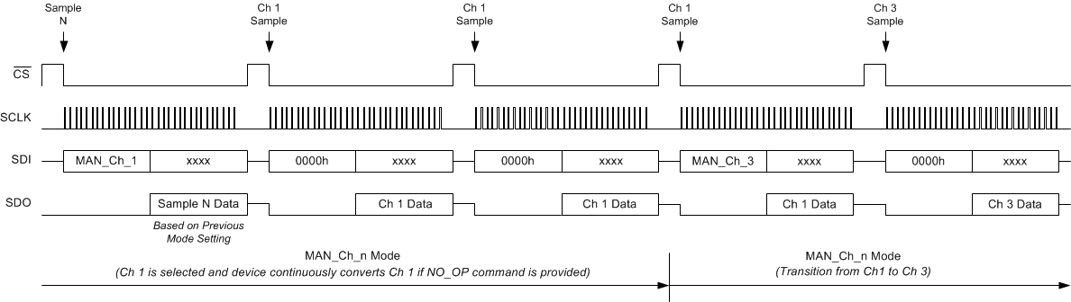 Figure 84. Device Operation in MAN_Ch_n Mode
8.4.2.7 Channel Sequencing Modes
The devices offer two channel sequencing modes: AUTO_RST and MAN_Ch_n.
In AUTO_RST mode, the channel number automatically increments in every subsequent frame. As explained in the Auto-Scan Sequencing Control Registers section, the analog inputs can be selected for an automatic scan with a register setting. The device automatically scans only the selected analog inputs in ascending order. The unselected analog input channels can also be powered down for optimizing power consumption in this mode of operation. The auto-mode sequence can be reset at any time during an automatic scan (using the AUTO_RST command). When the reset command is received, the ongoing auto-mode sequence is reset and restarts from the lowest selected channel in the sequence.
In MAN_Ch_n mode, the same input channel is selected during every data conversion frame. The input command words to select individual analog channels in MAN_Ch_n mode are listed in Table 6. If a particular input channel is selected during a data frame, then the analog inputs on the same channel are sampled during the next data frame. Figure 85 shows the SDI command sequence for transitions from AUTO_RST to MAN_Ch_n mode.
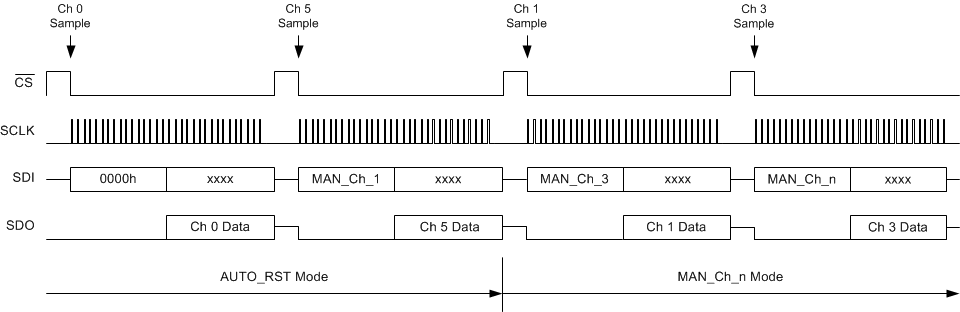 Figure 85. Transitioning from AUTO_RST to MAN_Ch_n Mode
 (Channels 0 and 5 are Selected for Auto Sequence)
Figure 86 shows the SDI command sequence for transitions from MAN_Ch_n to AUTO_RST mode. Note that each SDI command is executed on the next CS falling edge. A RST command can be issued at any instant during any channel sequencing mode, after which the device is placed into a default power-up state in the next data frame.
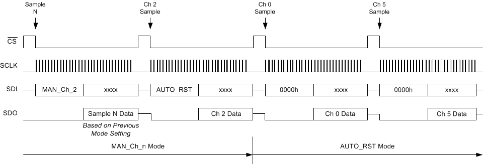 Figure 86. Transitioning from MAN_Ch_n to AUTO_RST Mode
(Channels 0 and 5 are Selected for Auto Sequence)
8.4.2.8 Reset Program Registers (RST)
The devices support a hardware and software reset (RST) mode in which all program registers are reset to their default values. The devices can be put into RST mode using a hardware pin, as explained in the RST/PD (Input) section.
The device program registers can be reset to their default values during any data frame by executing a valid write operation on the command register with a RST command of 8500h, as shown in Figure 87. The device remains in RST mode if no valid conversion command (AUTO_RST or MAN_Ch_n) is executed and SDI remains low (refer to the Continued Operation in the Selected Mode (NO_OP) section) during the subsequent data frames. When the device operates in RST mode, the program register settings can be updated, as explained in Program Register Read/Write Operation section using 16 SCLK cycles. However, if the user provides complete 32 SCLK cycles, then the SDO line yields all 1's on the last 16 SCLK cycles because there is no ongoing conversion in RST mode. The values of the program register can be read normally during this mode. A valid AUTO_RST or MAN_CH_n channel selection command must be executed for initiating a conversion on a particular analog channel using the default program register settings.
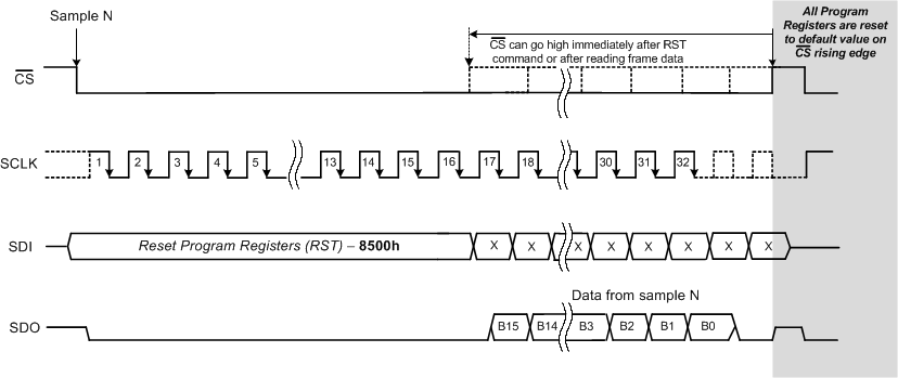 Figure 87. Reset Program Registers (RST) Timing Diagram
8.5 Register Map
The internal registers of the ADS8684 and ADS8688 are categorized into two categories: command registers and program registers.
The command registers are used to select the channel sequencing mode (AUTO_RST or MAN_Ch_n), configure the device in standby (STDBY) or power-down (PWR_DN) mode, and reset (RST) the program registers to their default values.
The program registers are used to select the sequence of channels for AUTO_RST mode, select the SDO output format, and control input range settings for individual channels.
8.5.1 Command Register Description
The command register is a 16-bit, write-only register that is used to set the operating modes of the ADS8684 and ADS8688. The settings in this register are used to select the channel sequencing mode (AUTO_RST or MAN_Ch_n), configure the device in standby (STDBY) or power-down (PWR_DN) mode, and reset (RST) the program registers to their default values. All command settings for this register are listed in Table 6. During power-up or reset, the default content of the command register is all 0's and the device waits for a command to be written before being placed into any mode of operation. Refer to Figure 1 for a typical timing diagram for writing a 16-bit command into the device. The device executes the command at the end of this particular data frame when the CS signal goes high.
Table 6. Command Register Map
| REGISTER | MSB BYTE | LSB BYTE | COMMAND (Hex) |
OPERATION IN NEXT FRAME | ||||||||||||||
|---|---|---|---|---|---|---|---|---|---|---|---|---|---|---|---|---|---|---|
| B15 | B14 | B13 | B12 | B11 | B10 | B9 | B8 | B[7:0] | ||||||||||
| Continued Operation (NO_OP) |
0 | 0 | 0 | 0 | 0 | 0 | 0 | 0 | 0000 0000 | 0000h | Continue operation in previous mode | |||||||
| Standby (STDBY) |
1 | 0 | 0 | 0 | 0 | 0 | 1 | 0 | 0000 0000 | 8200h | Device is placed into standby mode | |||||||
| Power Down (PWR_DN) |
1 | 0 | 0 | 0 | 0 | 0 | 1 | 1 | 0000 0000 | 8300h | Device is powered down | |||||||
| Reset program registers (RST) |
1 | 0 | 0 | 0 | 0 | 1 | 0 | 1 | 0000 0000 | 8500h | Program register is reset to default | |||||||
| Auto Ch. Sequence with Reset (AUTO_RST) |
1 | 0 | 1 | 0 | 0 | 0 | 0 | 0 | 0000 0000 | A000h | Auto mode enabled following a reset | |||||||
| Manual Ch 0 Selection (MAN_Ch_0) |
1 | 1 | 0 | 0 | 0 | 0 | 0 | 0 | 0000 0000 | C000h | Channel 0 input is selected | |||||||
| Manual Ch 1 Selection (MAN_Ch_1) |
1 | 1 | 0 | 0 | 0 | 1 | 0 | 0 | 0000 0000 | C400h | Channel 1 input is selected | |||||||
| Manual Ch 2 Selection (MAN_Ch_2) |
1 | 1 | 0 | 0 | 1 | 0 | 0 | 0 | 0000 0000 | C800h | Channel 2 input is selected | |||||||
| Manual Ch 3 Selection (MAN_Ch_3) |
1 | 1 | 0 | 0 | 1 | 1 | 0 | 0 | 0000 0000 | CC00h | Channel 3 input is selected | |||||||
| Manual Ch 4 Selection (MAN_Ch_4)(1) |
1 | 1 | 0 | 1 | 0 | 0 | 0 | 0 | 0000 0000 | D000h | Channel 4 input is selected | |||||||
| Manual Ch 5 Selection (MAN_Ch_5) |
1 | 1 | 0 | 1 | 0 | 1 | 0 | 0 | 0000 0000 | D400h | Channel 5 input is selected | |||||||
| Manual Ch 6 Selection (MAN_Ch_6) |
1 | 1 | 0 | 1 | 1 | 0 | 0 | 0 | 0000 0000 | D800h | Channel 6 input is selected | |||||||
| Manual Ch 7 Selection (MAN_Ch_7) |
1 | 1 | 0 | 1 | 1 | 1 | 0 | 0 | 0000 0000 | DC00h | Channel 7 input is selected | |||||||
| Manual AUX Selection (MAN_AUX) |
1 | 1 | 1 | 0 | 0 | 0 | 0 | 0 | 0000 0000 | E000h | AUX channel input is selected | |||||||
8.5.2 Program Register Description
The program register is a 16-bit register used to set the operating modes of the ADS8684 and ADS8688. The settings in this register are used to select the channel sequence for AUTO_RST mode, configure the device ID in daisy-chain mode, select the SDO output format, and control the input range settings for individual channels. All program settings for this register are listed in Table 9. During power-up or reset, the default content of the program register is all 0's and the device waits for a command to be written before being placed into any mode of operation.
8.5.2.1 Program Register Read/Write Operation
The program register is a 16-bit read or write register. There must be a minimum of 16 SCLKs after the CS falling edge for any read or write operation to the program registers. When CS goes low, the SDO line goes low as well. The device receives the command (as shown in Table 7 and Table 8) through SDI where the first seven bits (bits[15:9]) represent the register address and the eighth bit (bit 8) is the write or read instruction.
For a write cycle, the next eight bits (bits[7:0]) on the SDI are the desired data for the addressed register. A typical timing diagram for a program register write cycle is shown in Figure 88.
Table 7. Write Cycle Command Word
| PIN | REGISTER ADDRESS | WR/RD | DATA |
|---|---|---|---|
| BIT[15:9] | BIT 8 | BITS[7:0] | |
| SDI | ADDR[6:0] | 1 | DIN[7:0] |
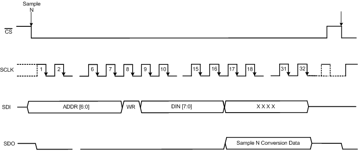 Figure 88. Timing Diagram Showing Program Register Write Cycle
For a read cycle, the next eight bits (bits[7:0]) in the SDI are don’t care bits. SDO outputs the 8-bit data from the addressed register during these eight clocks, in MSB-first fashion. A typical timing diagram for a program register read cycle is shown in Figure 89.
Table 8. Read Cycle Command Word
| PIN | REGISTER ADDRESS | WR/RD | DATA |
|---|---|---|---|
| BIT[15:9] | BIT 8 | BITS[7:0] | |
| SDI | ADDR[6:0] | 0 | XXXXX |
| SDO | 0000 000 | 0 | DOUT[7:0] |
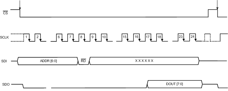 Figure 89. Program Register Read Cycle Timing Diagram
8.5.2.2 Program Register Map
This section provides a bit-by-bit description of each program register.
Table 9. Program Register Map
| REGISTER | REGISTER ADDRESS BITS[15:9] | DEFAULT VALUE(1) | BIT 7 | BIT 6 | BIT 5 | BIT 4 | BIT 3 | BIT 2 | BIT 1 | BIT 0 |
|---|---|---|---|---|---|---|---|---|---|---|
| AUTO SCAN SEQUENCING CONTROL | ||||||||||
| AUTO_SEQ_EN | 01h | FFh | CH7_EN(2) | CH6_EN | CH5_EN | CH4_EN | CH3_EN | CH2_EN | CH1_EN | CH0_EN |
| Channel Power Down | 02h | 00h | CH7_PD | CH6_PD | CH5_PD | CH4_PD | CH3_PD | CH2_PD | CH1_PD | CH0_PD |
| DEVICE FEATURES SELECTION CONTROL | ||||||||||
| Feature Select | 03h | 00h | DEV[1:0] | 1 | 0 | 1 | SDO [2:0] | |||
| RANGE SELECT REGISTERS | ||||||||||
| Channel 0 Input Range | 05h | 00h | 0 | 0 | 0 | 0 | 0 | Range Select Channel 0 [2:0] | ||
| Channel 1 Input Range | 06h | 00h | 0 | 0 | 0 | 0 | 0 | Range Select Channel 1 [2:0] | ||
| Channel 2 Input Range | 07h | 00h | 0 | 0 | 0 | 0 | 0 | Range Select Channel 2 [2:0] | ||
| Channel 3 Input Range | 08h | 00h | 0 | 0 | 0 | 0 | 0 | Range Select Channel 3 [2:0] | ||
| Channel 4 Input Range | 09h | 00h | 0 | 0 | 0 | 0 | 0 | Range Select Channel 4 [2:0] | ||
| Channel 5 Input Range | 0Ah | 00h | 0 | 0 | 0 | 0 | 0 | Range Select Channel 5 [2:0] | ||
| Channel 6 Input Range | 0Bh | 00h | 0 | 0 | 0 | 0 | 0 | Range Select Channel 6 [2:0] | ||
| Channel 7 Input Range | 0Ch | 00h | 0 | 0 | 0 | 0 | 0 | Range Select Channel 7 [2:0] | ||
| Ch 0 Hysteresis | 15h | 00h | CH0_HYST [7:0] | |||||||
| Ch 0 High Threshold MSB | 16h | FFh | CH0_HT [15:8] | |||||||
| Ch 0 High Threshold LSB | 17h | FFh | CH0_HT [7:0] | |||||||
| Ch 0 Low Threshold MSB | 18h | 00h | CH0_LT [15:8] | |||||||
| Ch 0 Low Threshold LSB | 19h | 00h | CH0_LT [7:0] | |||||||
| Ch 7 Hysteresis | 38h | 00h | CH7_HYST [7:0] | |||||||
| Ch 7 High Threshold MSB | 39h | FFh | CH7_HT [15:8] | |||||||
| Ch 7 High Threshold LSB | 3Ah | FFh | CH7_HT [7:0] | |||||||
| Ch 7 Low Threshold MSB | 3Bh | 00h | CH7_LT [15:8] | |||||||
| Ch 7 Low Threshold LSB | 3Ch | 00h | CH7_LT [7:0] | |||||||
| COMMAND READ BACK (Read-Only) | ||||||||||
| Command Read Back | 3Fh | 00h | COMMAND_WORD [7:0] | |||||||
8.5.2.3 Auto-Scan Sequencing Control Registers
In AUTO_RST mode, the device automatically scans the preselected channels in ascending order with a new channel selected for every conversion. Each individual channel can be selectively included in the auto channel sequencing. For the channels that are not selected for auto sequencing, the analog front-end circuitry can be individually powered down.
8.5.2.3.1 Auto-Scan Sequence Enable Register (address = 01h)
This register selects individual channels for sequencing in AUTO_RST mode. The default value for this register is FFh, which implies that in default condition all channels are included in the auto-scan sequence.
| 7 | 6 | 5 | 4 | 3 | 2 | 1 | 0 |
| CH7_EN(2) | CH6_EN | CH5_EN | CH4_EN | CH3_EN | CH2_EN | CH1_EN | CH0_EN |
| R/W | R/W | R/W | R/W | R/W | R/W | R/W | R/W |
| LEGEND: R/W = Read/Write |
Table 10. AUTO_SEQ_EN Field Descriptions
| Bit | Field | Type | Reset | Description |
|---|---|---|---|---|
| 7 | CH7_EN | R/W | 1h | Channel 7 enable. 0 = Channel 7 is not selected for sequencing in AUTO_RST mode 1 = Channel 7 is selected for sequencing in AUTO_RST mode |
| 6 | CH6_EN | R/W | 1h | Channel 6 enable. 0 = Channel 6 is not selected for sequencing in AUTO_RST mode 1 = Channel 6 is selected for sequencing in AUTO_RST mode |
| 5 | CH5_EN | R/W | 1h | Channel 5 enable. 0 = Channel 5 is not selected for sequencing in AUTO_RST mode 1 = Channel 5 is selected for sequencing in AUTO_RST mode |
| 4 | CH4_EN | R/W | 1h | Channel 4 enable. 0 = Channel 4 is not selected for sequencing in AUTO_RST mode 1 = Channel 4 is selected for sequencing in AUTO_RST mode |
| 3 | CH3_EN | R/W | 1h | Channel 3 enable. 0 = Channel 3 is not selected for sequencing in AUTO_RST mode 1 = Channel 3 is selected for sequencing in AUTO_RST mode |
| 2 | CH2_EN | R/W | 1h | Channel 2 enable. 0 = Channel 2 is not selected for sequencing in AUTO_RST mode 1 = Channel 2 is selected for sequencing in AUTO_RST mode |
| 1 | CH1_EN | R/W | 1h | Channel 1 enable. 0 = Channel 1 is not selected for sequencing in AUTO_RST mode 1 = Channel 1 is selected for sequencing in AUTO_RST mode |
| 0 | CH0_EN | R/W | 1h | Channel 0 enable. 0 = Channel 0 is not selected for sequencing in AUTO_RST mode 1 = Channel 0 is selected for sequencing in AUTO_RST mode |
8.5.2.3.2 Channel Power Down Register (address = 02h)
This register powers down individual channels that are not included for sequencing in AUTO_RST mode. The default value for this register is 00h, which implies that in default condition all channels are powered up.
| 7 | 6 | 5 | 4 | 3 | 2 | 1 | 0 |
| CH7_PD(2) | CH6_PD | CH5_PD | CH4_PD | CH3_PD | CH2_PD | CH1_PD | CH0_PD |
| R/W | R/W | R/W | R/W | R/W | R/W | R/W | R/W |
| LEGEND: R/W = Read/Write |
Table 11. Channel Power Down Register Field Descriptions
| Bit | Field | Type | Reset | Description |
|---|---|---|---|---|
| 7 | CH7_PD | R/W | 0h | Channel 7 power-down. 0 = The analog front-end on channel 7 is powered up and channel 7 can be included in the AUTO_RST sequence 1 = The analog front-end on channel 7 is powered down and channel 7 cannot be included in the AUTO_RST sequence |
| 6 | CH6_PD | R/W | 0h | Channel 6 power-down. 0 = The analog front-end on channel 6 is powered up and channel 6 can be included in the AUTO_RST sequence 1 = The analog front-end on channel 6 is powered down and channel 6 cannot be included in the AUTO_RST sequence |
| 5 | CH5_PD | R/W | 0h | Channel 5 power-down. 0 = The analog front-end on channel 5 is powered up and channel 5 can be included in the AUTO_RST sequence 1 = The analog front-end on channel 5 is powered down and channel 5 cannot be included in the AUTO_RST sequence |
| 4 | CH4_PD | R/W | 0h | Channel 4 power-down. 0 = The analog front-end on channel 4 is powered up and channel 4 can be included in the AUTO_RST sequence 1 = The analog front-end on channel 4 is powered down and channel 4 cannot be included in the AUTO_RST sequence |
| 3 | CH3_PD | R/W | 0h | Channel 3 power-down. 0 = The analog front-end on channel 3 is powered up and channel 3 can be included in the AUTO_RST sequence 1 = The analog front end on channel 3 is powered down and channel 3 cannot be included in the AUTO_RST sequence |
| 2 | CH2_PD | R/W | 0h | Channel 2 power-down. 0 = The analog front end on channel 2 is powered up and channel 2 can be included in the AUTO_RST sequence 1 = The analog front end on channel 2 is powered down and channel 2 cannot be included in the AUTO_RST sequence |
| 1 | CH1_PD | R/W | 0h | Channel 1 power-down. 0 = The analog front end on channel 1 is powered up and channel 1 can be included in the AUTO_RST sequence 1 = The analog front end on channel 1 is powered down and channel 1 cannot be included in the AUTO_RST sequence |
| 0 | CH0_PD | R/W | 0h | Channel 0 power-down. 0 = The analog front end on channel 0 is powered up and channel 0 can be included in the AUTO_RST sequence 1 = The analog front end on channel 0 is powered down and channel 0 cannot be included in the AUTO_RST sequence |
8.5.2.4 Device Features Selection Control Register (address = 03h)
The bits in this register can be used to configure the device ID for daisy-chain operation and configure the output bit format on SDO.
| 7 | 6 | 5 | 4 | 3 | 2 | 1 | 0 |
| DEV[1:0] | 1 | 0 | 1 | SDO[2:0] | |||
| R/W | R/W | R | R | R | R/W | R/W | R/W |
| LEGEND: R/W = Read/Write; R = Read only |
Table 12. Feature Select Register Field Descriptions
| Bit | Field | Type | Reset | Description |
|---|---|---|---|---|
| 7:6 | DEV[1:0] | R/W | 0h | Device ID bits. 00 = ID for device 0 in daisy-chain mode 01 = ID for device 1 in daisy-chain mode 10 = ID for device 2 in daisy-chain mode 11 = ID for device 3 in daisy-chain mode |
| 5 | 1 | R | 1h | Must always be set to 1 |
| 4 | 0 | R | 0h | Must always be set to 0 |
| 3 | 1 | R | 1h | Must always be set to 1 |
| 2:0 | SDO[2:0] | R/W | 0h | SDO data format bits (refer to Table 13). |
Table 13. Description of Program Register Bits for SDO Data Format
| SDO FORMAT SDO[2:0} |
BEGINNING OF THE OUTPUT BIT STREAM | OUTPUT FORMAT | |||||
|---|---|---|---|---|---|---|---|
| BITS[24:9] | BITS[8:5] | BITS[4:3] | BITS[2:0] | ||||
| 000 | 16th SCLK falling edge; no latency |
Conversion result for selected channel (MSB-first) | SDO pulled low | ||||
| 001 | 16th SCLK falling edge; no latency |
Conversion result for selected channel (MSB-first) | Channel address(1) | SDO pulled low | |||
| 010 | 16th SCLK falling edge; no latency |
Conversion result for selected channel (MSB-first) | Channel address(1) | Device address(1) | SDO pulled low | ||
| 011 | 16th SCLK falling edge; no latency |
Conversion result for selected channel (MSB-first) | Channel address(1) | Device address(1) | Input range (1) |
||
Table 14. Bit Description for the SDO Data
| BIT | BIT DESCRIPTION |
|---|---|
| 24:9 | 16 bits of conversion result for the channel represented in MSB-first format. |
| 8:5 | Four bits of channel address. 0000 = Channel 0 0001 = Channel 1 0010 = Channel 2 0011 = Channel 3 0100 = Channel 4 (valid only for the ADS8688) 0101 = Channel 5 (valid only for the ADS8688) 0110 = Channel 6 (valid only for the ADS8688) 0111 = Channel 7 (valid only for the ADS8688) |
| 4:3 | Two bits of device address (mainly useful in daisy-chain mode). |
| 2:0 | Three bits of input voltage range (refer to the Range Select Registers (address = 05h (channel 0), 06h (channel 1), 07h (channel 2), 08h (channel 3), 09h (channel 4), 0Ah (channel 5), 0Bh (channel 6), 0Ch (channel 7))). |
8.5.2.5 Range Select Registers (address = 05h (channel 0), 06h (channel 1), 07h (channel 2),
08h (channel 3), 09h (channel 4), 0Ah (channel 5), 0Bh (channel 6), 0Ch (channel 7))
These registers allow the selection of input ranges for all individual channels (n = 0 to 3 for ADS8684 and n = 0 to 7 for ADS8688). The default value for these registers is 00h.
| 7 | 6 | 5 | 4 | 3 | 2 | 1 | 0 |
| 0 | 0 | 0 | 0 | 0 | Range_CHn[2:0] | ||
| R | R | R | R | R | R/W | R/W | R/W |
| LEGEND: R/W = Read/Write; R = Read only |
Table 15. Channel n Input Range Registers Field Descriptions
| Bit | Field | Type | Reset | Description |
|---|---|---|---|---|
| 7:3 | 0 | R | 0h | Must always be set to 0 |
| 2:0 | Range_CHn[2:0] | R/W | 0h | Input range selection bits for channel n (n = 0 to 3 for ADS8684 and n = 0 to 7 for ADS8688). 000 = Input range is set to ±2.5 x VREF 001 = Input range is set to ±1.25 x VREF 010 = Input range is set to ±0.625 x VREF 101 = Input range is set to 0 to 2.5 x VREF 110 = Input range is set to 0 to 1.25 x VREF |
8.5.3 Command Read-Back Register (address = 3Fh)
This register allows the user to read the device mode of operation. On execution of this command, the device outputs the command word executed in the previous data frame. The output of the command register appears on SDO from the 16th falling edge onwards in an MSB-first format. All information regarding the command register is contained in the first eight bits and the last eight bits are 0 (refer to Table 6) so the user may stop the command read-back operation after the 24th SCLK cycle.
| 7 | 6 | 5 | 4 | 3 | 2 | 1 | 0 |
| COMMAND_WORD[15:8] | |||||||
| R | R | R | R | R | R | R | R |
| LEGEND: R = Read only |
Table 16. Command Read-Back Register Field Descriptions
| Bit | Field | Type | Reset | Description |
|---|---|---|---|---|
| 7:0 | COMMAND_WORD[15:8] | R | 0h | Command executed in previous data frame. |