ZHCSCR1B July   2014  – August 2014 ADS8684 , ADS8688

PRODUCTION DATA.  

  1. 特性
  2. 应用
  3. 说明
  4. 修订历史记录
  5. Device Comparison Table
  6. Pin Configuration and Functions
  7. Specifications
    1. 7.1 Absolute Maximum Ratings
    2. 7.2 Handling Ratings
    3. 7.3 Recommended Operating Conditions
    4. 7.4 Thermal Information
    5. 7.5 Electrical Characteristics
    6. 7.6 Timing Requirements: Serial Interface
    7. 7.7 Typical Characteristics
  8. Detailed Description
    1. 8.1 Overview
    2. 8.2 Functional Block Diagram
    3. 8.3 Feature Description
      1. 8.3.1  Analog Inputs
      2. 8.3.2  Analog Input Impedance
      3. 8.3.3  Input Overvoltage Protection Circuit
      4. 8.3.4  Programmable Gain Amplifier (PGA)
      5. 8.3.5  Second-Order, Low-Pass Filter (LPF)
      6. 8.3.6  ADC Driver
      7. 8.3.7  Multiplexer (MUX)
      8. 8.3.8  Reference
        1. 8.3.8.1 Internal Reference
        2. 8.3.8.2 External Reference
      9. 8.3.9  Auxiliary Channel
        1. 8.3.9.1 Input Driver for the AUX Channel
      10. 8.3.10 ADC Transfer Function
    4. 8.4 Device Functional Modes
      1. 8.4.1 Device Interface
        1. 8.4.1.1 Digital Pin Description
          1. 8.4.1.1.1 CS (Input)
          2. 8.4.1.1.2 SCLK (Input)
          3. 8.4.1.1.3 SDI (Input)
          4. 8.4.1.1.4 SDO (Output)
          5. 8.4.1.1.5 DAISY (Input)
          6. 8.4.1.1.6 RST/PD (Input)
        2. 8.4.1.2 Data Acquisition Example
        3. 8.4.1.3 Host-to-Device Connection Topologies
          1. 8.4.1.3.1 Daisy-Chain Topology
          2. 8.4.1.3.2 Star Topology
      2. 8.4.2 Device Modes
        1. 8.4.2.1 Continued Operation in the Selected Mode (NO_OP)
        2. 8.4.2.2 Frame Abort Condition (FRAME_ABORT)
        3. 8.4.2.3 STANDBY Mode (STDBY)
        4. 8.4.2.4 Power-Down Mode (PWR_DN)
        5. 8.4.2.5 Auto Channel Enable with Reset (AUTO_RST)
        6. 8.4.2.6 Manual Channel n Select (MAN_Ch_n)
        7. 8.4.2.7 Channel Sequencing Modes
        8. 8.4.2.8 Reset Program Registers (RST)
    5. 8.5 Register Map
      1. 8.5.1 Command Register Description
      2. 8.5.2 Program Register Description
        1. 8.5.2.1 Program Register Read/Write Operation
        2. 8.5.2.2 Program Register Map
        3. 8.5.2.3 Auto-Scan Sequencing Control Registers
          1. 8.5.2.3.1 Auto-Scan Sequence Enable Register (address = 01h)
          2. 8.5.2.3.2 Channel Power Down Register (address = 02h)
        4. 8.5.2.4 Device Features Selection Control Register (address = 03h)
        5. 8.5.2.5 Range Select Registers (address = 05h (channel 0), 06h (channel 1), 07h (channel 2), 08h (channel 3), 09h (channel 4), 0Ah (channel 5), 0Bh (channel 6), 0Ch (channel 7))
      3. 8.5.3 Command Read-Back Register (address = 3Fh)
  9. Application and Implementation
    1. 9.1 Application Information
    2. 9.2 Typical Applications
      1. 9.2.1 Phase-Compensated, 8-Channel, Multiplexed Data Acquisition System for Power Automation
        1. 9.2.1.1 Design Requirements
        2. 9.2.1.2 Detailed Design Procedure
        3. 9.2.1.3 Application Curve
      2. 9.2.2 16-Bit, 8-Channel, Integrated Analog Input Module for Programmable Logic Controllers (PLCs)
        1. 9.2.2.1 Design Requirements
        2. 9.2.2.2 Detailed Design Procedure
        3. 9.2.2.3 Application Curve
  10. 10Power-Supply Recommendations
  11. 11Layout
    1. 11.1 Layout Guidelines
    2. 11.2 Layout Example
  12. 12器件和文档支持
    1. 12.1 文档支持
      1. 12.1.1 相关文档 
    2. 12.2 相关链接
    3. 12.3 Trademarks
    4. 12.4 Electrostatic Discharge Caution
    5. 12.5 术语表
  13. 13机械封装和可订购信息

封装选项

机械数据 (封装 | 引脚)
散热焊盘机械数据 (封装 | 引脚)
订购信息

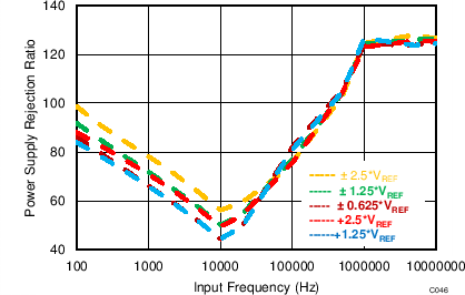
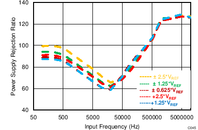
10 Power-Supply Recommendations

The device uses two separate power supplies: AVDD and DVDD. The internal circuits of the device operate on AVDD, while DVDD is used for the digital interface. AVDD and DVDD can be independently set to any value within the permissible range.

The AVDD supply pins must be decoupled with AGND by using a minimum 10-µF and 1-µF capacitor on each supply. Place the 1-µF capacitor as close to the supply pins as possible. Place a minimum 10-µF decoupling capacitor very close to the DVDD supply to provide the high-frequency digital switching current. The effect of using the decoupling capacitor is illustrated in the difference between the power-supply rejection ratio (PSRR) performance of the device. Figure 99 shows the PSRR of the device without using a decoupling capacitor. The PSRR improves when the decoupling capacitors are used, as shown in Figure 100.

C046_SBAS582.png
Code output near 32,769
Figure 99. PSRR Without a Decoupling Capacitor
C045_SBAS582.png
Code output near 32,768
Figure 100. PSRR With a Decoupling Capacitor