ZHCSCR1B July 2014 – August 2014 ADS8684 , ADS8688
PRODUCTION DATA.
- 1 特性
- 2 应用
- 3 说明
- 4 修订历史记录
- 5 Device Comparison Table
- 6 Pin Configuration and Functions
- 7 Specifications
-
8 Detailed Description
- 8.1 Overview
- 8.2 Functional Block Diagram
- 8.3 Feature Description
- 8.4
Device Functional Modes
- 8.4.1 Device Interface
- 8.4.2
Device Modes
- 8.4.2.1 Continued Operation in the Selected Mode (NO_OP)
- 8.4.2.2 Frame Abort Condition (FRAME_ABORT)
- 8.4.2.3 STANDBY Mode (STDBY)
- 8.4.2.4 Power-Down Mode (PWR_DN)
- 8.4.2.5 Auto Channel Enable with Reset (AUTO_RST)
- 8.4.2.6 Manual Channel n Select (MAN_Ch_n)
- 8.4.2.7 Channel Sequencing Modes
- 8.4.2.8 Reset Program Registers (RST)
- 8.5
Register Map
- 8.5.1 Command Register Description
- 8.5.2
Program Register Description
- 8.5.2.1 Program Register Read/Write Operation
- 8.5.2.2 Program Register Map
- 8.5.2.3 Auto-Scan Sequencing Control Registers
- 8.5.2.4 Device Features Selection Control Register (address = 03h)
- 8.5.2.5 Range Select Registers (address = 05h (channel 0), 06h (channel 1), 07h (channel 2), 08h (channel 3), 09h (channel 4), 0Ah (channel 5), 0Bh (channel 6), 0Ch (channel 7))
- 8.5.3 Command Read-Back Register (address = 3Fh)
- 9 Application and Implementation
- 10Power-Supply Recommendations
- 11Layout
- 12器件和文档支持
- 13机械封装和可订购信息
11 Layout
11.1 Layout Guidelines
Figure 101 illustrates a PCB layout example for the ADS8684 and ADS8688.
- Partition the PCB into analog and digital sections. Care must be taken to ensure that the analog signals are kept away from the digital lines. This layout helps keep the analog input and reference input signals away from the digital noise. In this layout example, the analog input and reference signals are routed on the lower side of the board while the digital connections are routed on the top side of the board.
- Using a single dedicated ground plane is strongly encouraged.
- Power sources to the ADS8684 and ADS8688 must be clean and well-bypassed. TI recommends using a
1-μF, X7R-grade, 0603-size ceramic capacitor with at least a 10-V rating in close proximity to the analog (AVDD) supply pins. For decoupling the digital (DVDD) supply pin, a 10-μF, X7R-grade, 0805-size ceramic capacitor with at least a 10-V rating is recommended. Placing vias between the AVDD, DVDD pins and the bypass capacitors must be avoided. All ground pins must be connected to the ground plane using short, low impedance paths. - There are two decoupling capacitors used for REFCAP pin. The first is a small, 1-μF, X7R-grade, 0603-size ceramic capacitor placed close to the device pins for decoupling the high-frequency signals and the second is a 22-µF, X7R-grade, 1210-size ceramic capacitor to provide the charge required by the reference circuit of the device. Both these capacitors must be directly connected to the device pins without any vias between the pins and capacitors.
- The REFIO pin also must be decoupled with a 10-µF ceramic capacitor, if the internal reference of the device is used. The capacitor must be placed close to the device pins.
- For the auxiliary channel, the fly-wheel RC filter components must be placed close to the device. Among ceramic surface-mount capacitors, COG (NPO) ceramic capacitors provide the best capacitance precision. The type of dielectric used in COG (NPO) ceramic capacitors provides the most stable electrical properties over voltage, frequency, and temperature changes.
11.2 Layout Example
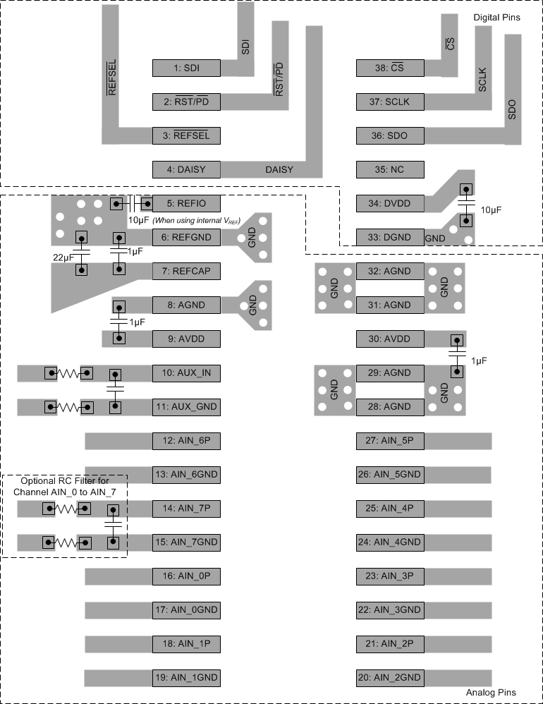 Figure 101. Board Layout for ADS8684 and ADS8688