ZHCSCR1B July 2014 – August 2014 ADS8684 , ADS8688
PRODUCTION DATA.
- 1 特性
- 2 应用
- 3 说明
- 4 修订历史记录
- 5 Device Comparison Table
- 6 Pin Configuration and Functions
- 7 Specifications
-
8 Detailed Description
- 8.1 Overview
- 8.2 Functional Block Diagram
- 8.3 Feature Description
- 8.4
Device Functional Modes
- 8.4.1 Device Interface
- 8.4.2
Device Modes
- 8.4.2.1 Continued Operation in the Selected Mode (NO_OP)
- 8.4.2.2 Frame Abort Condition (FRAME_ABORT)
- 8.4.2.3 STANDBY Mode (STDBY)
- 8.4.2.4 Power-Down Mode (PWR_DN)
- 8.4.2.5 Auto Channel Enable with Reset (AUTO_RST)
- 8.4.2.6 Manual Channel n Select (MAN_Ch_n)
- 8.4.2.7 Channel Sequencing Modes
- 8.4.2.8 Reset Program Registers (RST)
- 8.5
Register Map
- 8.5.1 Command Register Description
- 8.5.2
Program Register Description
- 8.5.2.1 Program Register Read/Write Operation
- 8.5.2.2 Program Register Map
- 8.5.2.3 Auto-Scan Sequencing Control Registers
- 8.5.2.4 Device Features Selection Control Register (address = 03h)
- 8.5.2.5 Range Select Registers (address = 05h (channel 0), 06h (channel 1), 07h (channel 2), 08h (channel 3), 09h (channel 4), 0Ah (channel 5), 0Bh (channel 6), 0Ch (channel 7))
- 8.5.3 Command Read-Back Register (address = 3Fh)
- 9 Application and Implementation
- 10Power-Supply Recommendations
- 11Layout
- 12器件和文档支持
- 13机械封装和可订购信息
7 Specifications
7.1 Absolute Maximum Ratings
over operating free-air temperature range (unless otherwise noted)(1)| MIN | MAX | UNIT | |
|---|---|---|---|
| AIN_nP to AIN_nGND(2) | –20 | 20 | V |
| AIN_nP to AIN_nGND(3) | –11 | 11 | V |
| AIN_nGND to GND | –0.3 | 0.3 | V |
| AUX_IN to GND | –0.3 | AVDD + 0.3 | V |
| AVDD to GND or DVDD to GND | –0.3 | 7 | V |
| REFCAP to REFGND or REFIO to REFGND | –0.3 | 5.7 | V |
| GND to REFGND | –0.3 | 0.3 | V |
| Digital input pins to GND | –0.3 | DVDD + 0.3 | V |
| Digital output pins to GND | –0.3 | DVDD + 0.3 | V |
| Operating temperature range, TA | –40 | 125 | °C |
(1) Stresses beyond those listed under Absolute Maximum Ratings may cause permanent damage to the device. These are stress ratings only, and do not imply functional operation of the device at these or any other conditions beyond those indicated under Recommended Operating Conditions. Exposure to absolute-maximum-rated conditions for extended periods may affect device reliability.
(2) AVDD = 5 V or offers a low impedance of < 30 kΩ.
(3) AVDD = floating with an impedance > 30 kΩ.
7.2 Handling Ratings
| MIN | MAX | UNIT | ||||
|---|---|---|---|---|---|---|
| Tstg | Storage temperature range | –65 | 150 | °C | ||
| V(ESD) | Electrostatic discharge | Human body model (HBM), per ANSI/ESDA/JEDEC JS-001, all pins(1) | Analog input pins (AIN_nP; AIN_nGND) | –4000 | 4000 | V |
| All other pins | –2000 | 2000 | ||||
| Charged device model (CDM), per JEDEC specification JESD22-C101, all pins(2) | –500 | 500 | ||||
(1) JEDEC document JEP155 states that 500-V HBM allows safe manufacturing with a standard ESD control process.
(2) JEDEC document JEP157 states that 250-V CDM allows safe manufacturing with a standard ESD control process.
7.3 Recommended Operating Conditions
over operating free-air temperature range (unless otherwise noted)| MIN | NOM | MAX | UNIT | ||
|---|---|---|---|---|---|
| AVDD | Analog supply voltage | 4.75 | 5 | 5.25 | V |
| DVDD | Digital supply voltage | 1.65 | 3.3 | AVDD | V |
7.4 Thermal Information
| THERMAL METRIC(1) | ADS8684, ADS8688 | UNIT | |
|---|---|---|---|
| TSSOP (PW) | |||
| 38 PINS | |||
| RθJA | Junction-to-ambient thermal resistance | 68.8 | °C/W |
| RθJC(top) | Junction-to-case (top) thermal resistance | 19.9 | |
| RθJB | Junction-to-board thermal resistance | 30.4 | |
| ψJT | Junction-to-top characterization parameter | 1.3 | |
| ψJB | Junction-to-board characterization parameter | 29.8 | |
| RθJC(bot) | Junction-to-case (bottom) thermal resistance | NA | |
(1) For more information about traditional and new thermal metrics, see the IC Package Thermal Metrics application report, SPRA953.
7.5 Electrical Characteristics
Minimum and maximum specifications are at TA = –40°C to 125°C. Typical specifications are at TA = 25°C.AVDD = 5 V, DVDD = 3 V, VREF = 4.096 V (internal), and fSAMPLE = 500 kSPS, unless otherwise noted.
| PARAMETER | TEST CONDITIONS | MIN | TYP | MAX | UNIT | TEST(1) LEVEL | |||
|---|---|---|---|---|---|---|---|---|---|
| ANALOG INPUTS | |||||||||
| Full-scale input span(2)
(AIN_nP to AIN_nGND) |
Input range = ±2.5 × VREF | –2.5 × VREF | 2.5 × VREF | V | A | ||||
| Input range = ±1.25 × VREF | –1.25 × VREF | 1.25 × VREF | V | A | |||||
| Input range = ±0.625 × VREF | –0.625 × VREF | 0.625 × VREF | V | A | |||||
| Input range = 2.5 × VREF | 0 | 2.5 × VREF | V | A | |||||
| Input range = 1.25 × VREF | 0 | 1.25 × VREF | V | A | |||||
| AIN_nP | Operating input range, positive input |
Input range = ±2.5 × VREF | –2.5 × VREF | 2.5 × VREF | V | A | |||
| Input range = ±1.25 × VREF | –1.25 × VREF | 1.25 × VREF | V | A | |||||
| Input range = ±0.625 × VREF | –0.625 × VREF | 0.625 × VREF | V | A | |||||
| Input range = 2.5 × VREF | 0 | 2.5 × VREF | V | A | |||||
| Input range = 1.25 × VREF | 0 | 1.25 × VREF | V | A | |||||
| AIN_nGND | Operating input range, negative input | All input ranges | –0.1 | 0 | 0.1 | V | B | ||
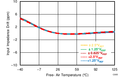
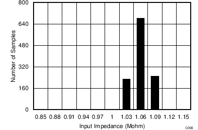
| zi | Input impedance | At TA = 25°C | 0.85 | 1 | 1.15 | MΩ | B | ||
| Input impedance drift | 7 | 25 | ppm/°C | B | |||||
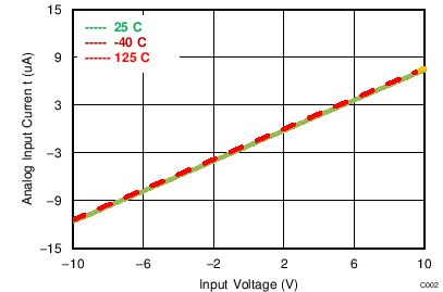
| IIkg(in) | Input leakage current | With voltage at AIN_nP pin = VIN, input range = ±2.5 × VREF |
VIN – 2.25 ———— RIN |
µA | A | ||||
| With voltage at AIN_nP pin = VIN, input range = ±1.25 × VREF |
VIN – 2.00 ———— RIN |
µA | A | ||||||
| With voltage at AIN_nP pin = VIN, input range = ±0.625 × VREF |
VIN – 1.60 ———— RIN |
µA | A | ||||||
| With voltage at AIN_nP pin = VIN, input range = 2.5 × VREF |
VIN – 2.50 ———— RIN |
µA | A | ||||||
| With voltage at AIN_nP pin = VIN, input range = 1.25 × VREF |
VIN – 2.50 ———— RIN |
µA | A | ||||||
| INPUT OVERVOLTAGE PROTECTION | |||||||||
| VOVP | Overvoltage protection voltage | AVDD = 5 V or offers low impedance < 30 kΩ, all input ranges |
–20 | 20 | V | B | |||
| AVDD = floating with impedance > 30 kΩ, all input ranges |
–11 | 11 | V | B | |||||
| SYSTEM PERFORMANCE | |||||||||
| Resolution | 16 | Bits | A | ||||||
| NMC | No missing codes | 16 | Bits | A | |||||
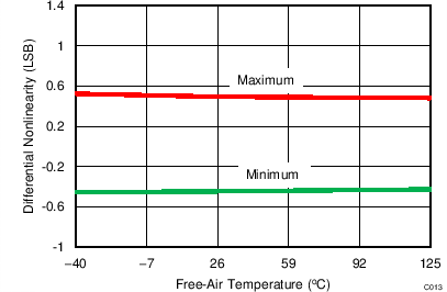
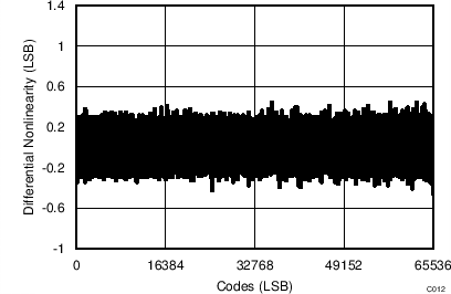
| DNL | Differential nonlinearity | –0.99 | ±0.5 | 1.5 | LSB(3) | A | |||
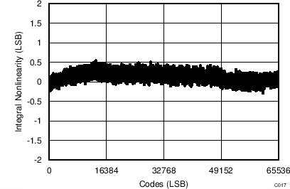
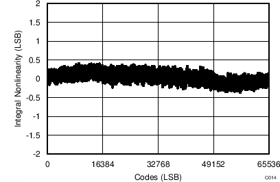
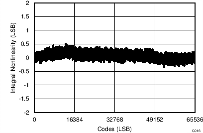
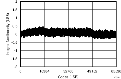
| INL | Integral nonlinearity(6) | –2 | ±0.75 | 2 | LSB | A | |||
| EG | Gain error | At TA = 25°C, all input ranges | ±0.02 | ±0.05 | %FSR(4) | A | |||
| Gain error matching (channel-to-channel) |
At TA = 25°C, all input ranges | ±0.02 | ±0.05 | %FSR | A | ||||
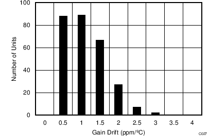
| Gain error temperature drift | All input ranges | ±1 | ±4 | ppm/°C | B | ||||
| EO | Offset error | At TA = 25°C, input range = ±2.5 × VREF |
±0.5 | ±0.75 | mV | A | |||
| At TA = 25°C, input range = ±1.25 × VREF |
±0.5 | ±1 | mV | A | |||||
| At TA = 25°C, input range = ±0.625 × VREF |
±0.5 | ±1.5 | mV | A | |||||
| At TA = 25°C, input range = 0 to 2.5 × VREF |
±0.5 | ±2 | mV | A | |||||
| At TA = 25°C, input range = 0 to 1.25 × VREF |
±0.5 | ±2 | mV | A | |||||
| Offset error matching (channel-to-channel) |
At TA = 25°C, input range = ±2.5 × VREF |
±0.5 | ±0.75 | mV | A | ||||
| At TA = 25°C, input range = ±1.25 × VREF |
±0.5 | ±1 | mV | A | |||||
| At TA = 25°C, input range = ±0.625 × VREF |
±0.5 | ±1.5 | mV | A | |||||
| At TA = 25°C, input range = 0 to 2.5 × VREF |
±0.5 | ±2 | mV | A | |||||
| At TA = 25°C, input range = 0 to 1.25 × VREF |
±0.5 | ±2 | mV | A | |||||
| Offset error temperature drift | All input ranges | ±1 | ±3 | ppm/°C | B | ||||
| SAMPLING DYNAMICS | |||||||||
| tCONV | Conversion time | 850 | ns | A | |||||
| tACQ | Acquisition time | 1150 | ns | A | |||||
| fS | Maximum throughput rate without latency |
500 | kSPS | A | |||||
| DYNAMIC CHARACTERISTICS | |||||||||
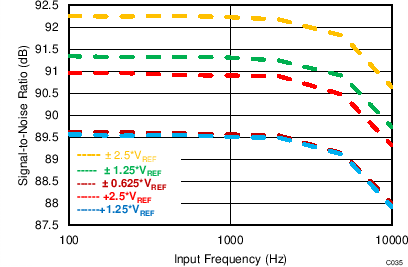
| SNR | Signal-to-noise ratio (VIN – 0.5 dBFS at 1 kHz) |
Input range = ±2.5 × VREF | 90 | 92 | dB | A | |||
| Input range = ±1.25 × VREF | 89 | 91 | dB | A | |||||
| Input range = ±0.625 × VREF | 87.5 | 89 | dB | A | |||||
| Input range = 2.5 × VREF | 88.5 | 90.5 | dB | A | |||||
| Input range = 1.25 × VREF | 87.5 | 89 | dB | A | |||||
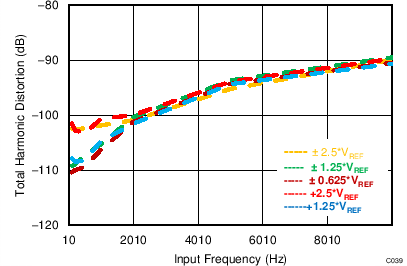
| THD | Total harmonic distortion(5)
(VIN – 0.5 dBFS at 1 kHz) |
All input ranges | –102 | dB | B | ||||
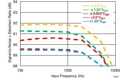
| SINAD | Signal-to-noise + distortion (VIN – 0.5 dBFS at 1 kHz) |
Input range = ±2.5 × VREF | 89 | 91.5 | dB | A | |||
| Input range = ±1.25 × VREF | 88.5 | 91 | dB | A | |||||
| Input range = ±0.625 × VREF | 87 | 89 | dB | A | |||||
| Input range = 2.5 × VREF | 87.5 | 90.5 | dB | A | |||||
| Input range = 1.25 × VREF | 87 | 89 | dB | A | |||||
| SFDR | Spurious-free dynamic range (VIN – 0.5 dBFS at 1 kHz) |
All input ranges | 103 | dB | B | ||||
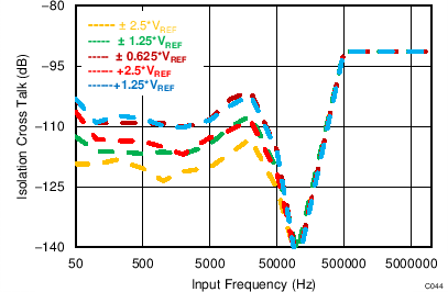
| Crosstalk isolation(7) | Aggressor channel input is overdriven to 2 × maximum input voltage | 110 | dB | B | |||||
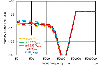
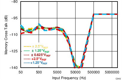
| Crosstalk memory(8) | Aggressor channel input is overdriven to 2 × maximum input voltage | 90 | dB | B | |||||
| BW(–3 dB) | Small-signal bandwidth | –3 dB | At TA = 25°C, all input ranges | 15 | kHz | B | |||
| BW(–0.1 dB) | –0.1 dB | At TA = 25°C, all input ranges | 2.5 | kHz | B | ||||
| AUXILIARY CHANNEL | |||||||||
| Resolution | 16 | Bits | A | ||||||
| V(AUX_IN) | AUX_IN voltage range | (AUX_IN – AUX_GND) | 0 | VREF | V | A | |||
| Operating input range | AUX_IN | 0 | VREF | V | A | ||||
| AUX_GND | 0 | V | A | ||||||
| Ci | Input capacitance | During sampling | 75 | pF | C | ||||
| During conversion | 5 | pF | C | ||||||
| IIkg(in) | Input leakage current | 100 | nA | A | |||||
| DNL | Differential nonlinearity | –0.99 | ±0.6 | 1.5 | LSB | A | |||
| INL | Integral nonlinearity | –4 | ±1.5 | 4 | LSB | A | |||
| EG(AUX) | Gain error | At TA = 25°C | ±0.02 | ±0.2 | % FSR | A | |||
| EO(AUX) | Offset error | At TA = 25°C | –10 | 10 | mV | A | |||
| SNR | Signal-to-noise ratio | V(AUX_IN) = –0.5 dBFS at 1 kHz | 87 | 88 | dB | A | |||
| THD | Total harmonic distortion(5) | V(AUX_IN) = –0.5 dBFS at 1 kHz | –102 | dB | B | ||||
| SINAD | Signal-to-noise + distortion | V(AUX_IN) = –0.5 dBFS at 1 kHz | 86 | 88 | dB | A | |||
| SFDR | Spurious-free dynamic range | V(AUX_IN) = –0.5 dBFS at 1 kHz | 102 | dB | B | ||||
| INTERNAL REFERENCE OUTPUT | |||||||||
| V(REFIO_INT)(9) | Voltage on REFIO pin (configured as output) |
At TA = 25°C | 4.095 | 4.096 | 4.097 | V | A | ||
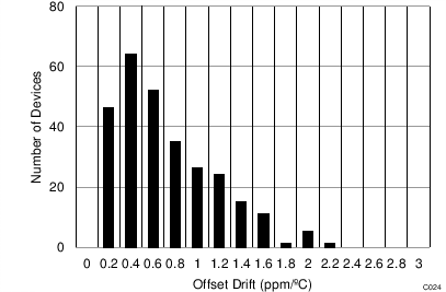
| Internal reference temperature drift | 6 | 10 | ppm/°C | B | |||||
| C(OUT_REFIO) | Decoupling capacitor on REFIO | 10 | 22 | µF | B | ||||
| V(REFCAP) | Reference voltage to ADC (on REFCAP pin) |
At TA = 25°C | 4.095 | 4.096 | 4.097 | V | A | ||
| Reference buffer output impedance | 0.5 | 1 | Ω | B | |||||
| Reference buffer temperature drift | 0.6 | 1.5 | ppm/°C | B | |||||
| C(OUT_REFCAP) | Decoupling capacitor on REFCAP | 10 | 22 | μF | B | ||||
| Turn-on time | C(OUT_REFCAP) = 22 µF C(OUT_REFIO) = 22 µF |
15 | ms | B | |||||
| EXTERNAL REFERENCE INPUT | |||||||||
| VREFIO_EXT | External reference voltage on REFIO (configured as input) | 4.046 | 4.096 | 4.146 | V | C | |||
| POWER-SUPPLY REQUIREMENTS | |||||||||
| AVDD | Analog power-supply voltage | Analog supply | 4.75 | 5 | 5.25 | V | B | ||
| DVDD | Digital power-supply voltage | Digital supply range | 1.65 | 3.3 | AVDD | V | B | ||
| Digital supply range for specified performance | 2.7 | 3.3 | 5.25 | V | B | ||||
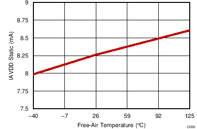
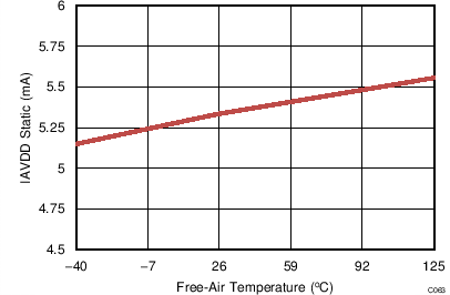
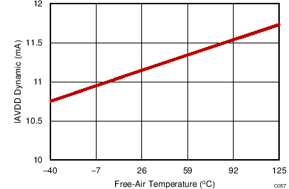
| IAVDD_DYN | Analog supply current | Dynamic, AVDD | For ADS8688; AVDD = 5 V, fS = maximum and internal reference | 13 | 16 | mA | A | ||
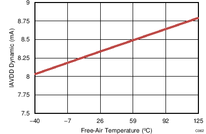
| For ADS8684; AVDD = 5 V, fS = maximum and internal reference | 8.5 | 11.5 | mA | A | |||||
| IAVDD_STC | Static | For ADS8688; AVDD = 5 V, device not converting and internal reference | 10 | 12 | mA | A | |||
| For ADS8684; AVDD = 5 V, device not converting and internal reference | 5.5 | 8.5 | mA | A | |||||
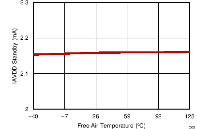
| ISTDBY | Power-down | At AVDD = 5 V, device in STDBY mode and internal reference | 3 | 4.5 | mA | A | |||
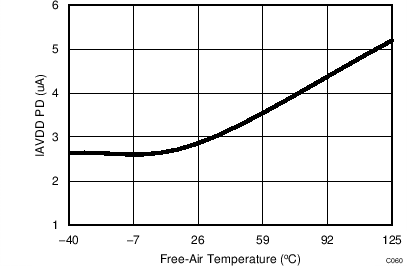
| IPWR_DN | Dynamic, DVDD | At AVDD = 5 V, device in PWR_DN | 3 | 20 | μA | B | |||
| IDVDD_DYN | Digital supply current | At DVDD = 3.3 V, output = 0000h | 0.5 | mA | A | ||||
| DIGITAL INPUTS (CMOS) | |||||||||
| VIH | Digital input logic levels DVDD > 2.1 V |
0.7 × DVDD | DVDD + 0.3 | V | A | ||||
| VIL | –0.3 | 0.3 × DVDD | V | A | |||||
| VIH | Digital input logic levels DVDD ≤ 2.1 V |
0.8 × DVDD | DVDD + 0.3 | V | A | ||||
| VIL | –0.3 | 0.2 × DVDD | V | A | |||||
| Input leakage current | 100 | nA | A | ||||||
| Input pin capacitance | 5 | pF | C | ||||||
| DIGITAL OUTPUTS (CMOS) | |||||||||
| VOH | Digital output logic levels | IO = 500-μA source | 0.8 × DVDD | DVDD | V | A | |||
| VOL | IO = 500-μA sink | 0 | 0.2 × DVDD | V | A | ||||
| Floating state leakage current | Only for SDO | 1 | µA | A | |||||
| Internal pin capacitance | 5 | pF | C | ||||||
| TEMPERATURE RANGE | |||||||||
| TA | Operating free-air temperature | –40 | 125 | °C | B | ||||
(1) Test Levels: (A) Tested at final test. Over temperature limits are set by characterization and simulation. (B) Limits set by characterization and simulation, across temperature range. (C) Typical value only for information, provided by design simulation.
(2) Ideal input span, does not include gain or offset error.
(3) LSB = least significant bit.
(4) FSR = full-scale range.
(5) Calculated on the first nine harmonics of the input frequency.
(6) This parameter is the endpoint INL, not best fit INL.
(7) Isolation crosstalk is measured by applying a full-scale sinusoidal signal up to 10 kHz to a channel, not selected in the multiplexing sequence, and measuring its effect on the output of any selected channel.
(8) Memory crosstalk is measured by applying a full-scale sinusoidal signal up to 10 kHz to a channel, which is selected in the multiplexing sequence, and measuring its effect on the output of the next selected channel, for all combinations of input channels.
(9) Does not include the variation in voltage resulting from solder shift effects.
7.6 Timing Requirements: Serial Interface
Minimum and maximum specifications are at TA = –40°C to 125°C. Typical specifications are at TA = 25°C.AVDD = 5 V, DVDD = 3 V, VREF = 4.096 V (internal), SDO load = 20 pF, and fSAMPLE = 500 kSPS, unless otherwise noted.
| PARAMETER | TEST CONDITION | MIN | TYP | MAX | UNIT | |
|---|---|---|---|---|---|---|
| TIMING SPECIFICATIONS | ||||||
| fS | Sampling frequency | fCLK = max | 500 | kSPS | ||
| tS | ADC cycle time period | fCLK = max | 2 | µs | ||
| fSCLK | Serial clock frequency | fS = max | 17 | MHz | ||
| tSCLK | Serial clock time period | fS = max | 59 | ns | ||
| tCONV | Conversion time | 850 | ns | |||
| tDV_CSDO | Delay time: CS falling to data enable | 10 | ns | |||
| tD_CKCS | Delay time: last SCLK falling to CS rising | 10 | ns | |||
| tDZ_CSDO | Delay time: CS rising to SDO going to 3-state | 10 | ns | |||
| TIMING REQUIREMENTS | ||||||
| tACQ | Acquisition time | 1150 | ns | |||
| tPH_CK | Clock high time | 0.4 | 0.6 | tSCLK | ||
| tPL_CK | Clock low time | 0.4 | 0.6 | tSCLK | ||
| tPH_CS | CS high time | 30 | ns | |||
| tSU_CSCK | Setup time: CS falling to SCLK falling | 30 | ns | |||
| tHT_CKDO | Hold time: SCLK falling to (previous) data valid on SDO | 10 | ns | |||
| tSU_DOCK | Setup time: SDO data valid to SCLK falling | 25 | ns | |||
| tSU_DICK | Setup time: SDI data valid to SCLK falling | 5 | ns | |||
| tHT_CKDI | Hold time: SCLK falling to (previous) data valid on SDI | 5 | ns | |||
| tSU_DSYCK | Setup time: DAISY data valid to SCLK falling | 5 | ns | |||
| tHT_CKDSY | Hold time: SCLK falling to (previous) data valid on DAISY | 5 | ns | |||
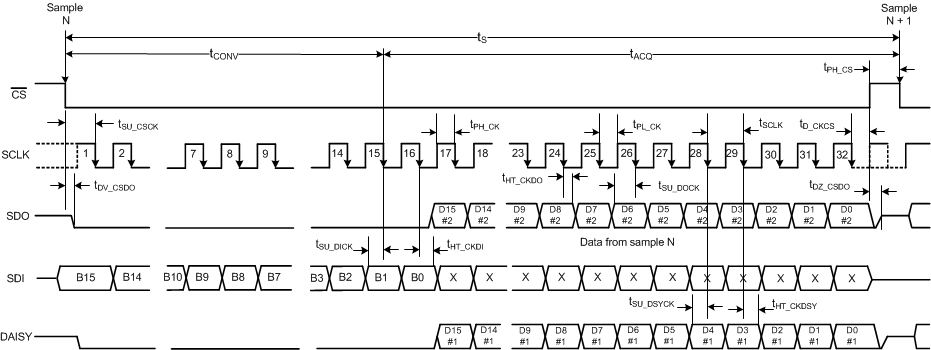 Figure 1. Serial Interface Timing Diagram
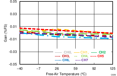
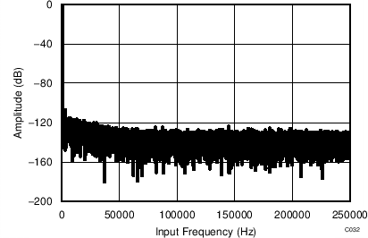
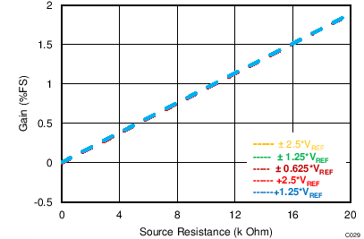
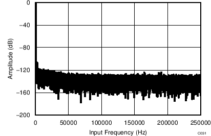
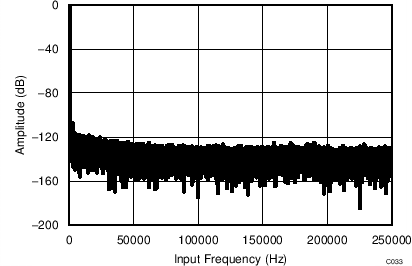
7.7 Typical Characteristics
At TA = 25°C, AVDD = 5 V, DVDD = 3 V, internal reference VREF = 4.096 V, and fSAMPLE = 500 kSPS, unless otherwise noted.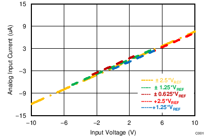
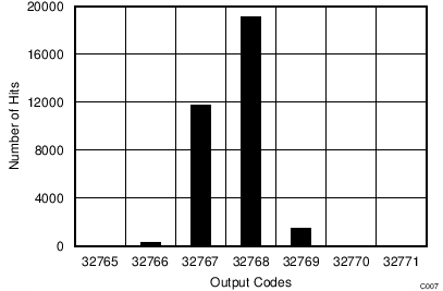
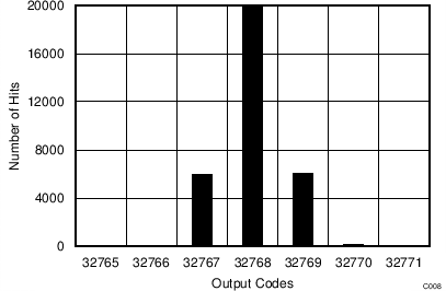
| Mean = 32767.8, Sigma = 0.58, Input = 0 V, Range = ±2.5 × VREF |
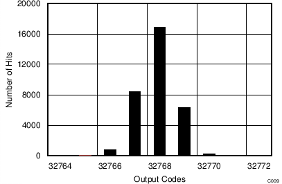
| Mean = 32767.932767.9(TBD), Sigma = 0.76, Input = 0 V, Range = ±0.625 × VREF |
| Mean = 32768.90, Sigma = 0.75, Input = 0.625 × VREF, Range = 1.25 × VREF |
| All input ranges |

| Range = ±1.25 × VREF |
| Range = 2.5 × VREF |
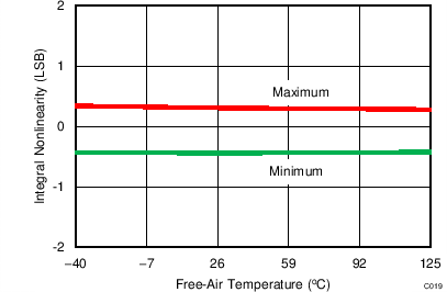
| Range = ±2.5 × VREF |
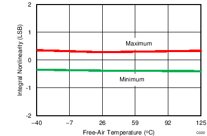
| Range = ±0.625 × VREF |
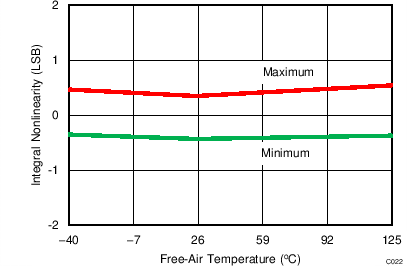
| Range = 1.25 × VREF |
| Range = ±2.5 × VREF |
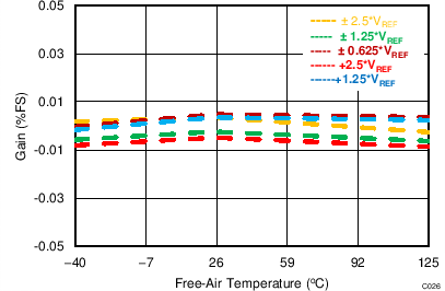
| Range = ±2.5 × VREF |
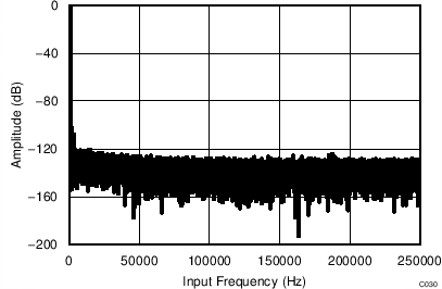
| Number of points = 64k, fIN = 1 kHz, SNR = 92.3 dB, SINAD = 91.9 dB, THD = 101 dB, SFDR = 104 dB |
| Number of points = 64k, fIN = 1 kHz, SNR = 89.6 dB, SINAD = 89.5 dB, THD = 106 dB, SFDR = 107 dB |

| Number of points = 64k, fIN = 1 kHz, SNR = 89.55 dB, SINAD = 89.4 dB, THD = 104 dB, SFDR = 107 dB |
| fIN = 1 kHz |
| fIN = 1 kHz |
| fIN = 1 kHz |
| Input = 2 × maximum input voltage |
Overrange Inputs
(During Sampling)
(During Sampling)
(Power Down)
| Input range = ±2.5 × VREF |
| Number of samples = 1160 |
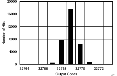
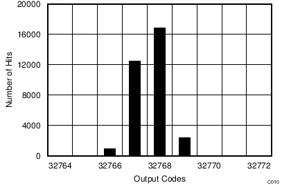
| Mean = 32768.1, Sigma = 0.63, Input = 0 V, Range = ±1.25 × VREF |
| Mean = 32767.75, Sigma = 0.65, Input = 1.25 × VREF, Range = 2.5 × VREF |
| All input ranges | ||
| Range = ±2.5 × VREF |
| Range = ±0.625 × VREF |
| Range = 1.25 × VREF |
| Range = ±1.25 × VREF |
| Range = 2.5 × VREF |
| Range = ±2.5 × VREF |
| Range = ±2.5 × VREF |
| Number of points = 64k, fIN = 1 kHz, SNR = 91.4 dB, SINAD = 91.2 dB, THD = 105 dB, SFDR = 107 dB |
| Number of points = 64k, fIN = 1 kHz, SNR = 90.93 dB, SINAD = 90.48 dB, THD = 100 dB, SFDR = 102 dB |
| Input = 2 × maximum input voltage |
Overrange Inputs
(fS = 500 kSPS)
(fS = 500 kSPS)
(STANDBY)