SBAS523D October 2010 – September 2017 ADS7223 , ADS7263 , ADS8363
PRODUCTION DATA.
- 1 Features
- 2 Applications
- 3 Description
- 4 Revision History
- 5 Device Comparison Table
- 6 Pin Configuration and Functions
-
7 Specifications
- 7.1 Absolute Maximum Ratings
- 7.2 ESD Ratings
- 7.3 Recommended Operating Conditions
- 7.4 Thermal Information
- 7.5 Electrical Characteristics: General
- 7.6 Electrical Characteristics: ADS8363
- 7.7 Electrical Characteristics: ADS7263
- 7.8 Electrical Characteristics: ADS7223
- 7.9 Switching Characteristics
- 7.10 Typical Characteristics
- 8 Detailed Description
- 9 Application and Implementation
- 10Power Supply Recommendations
- 11Layout
- 12Device and Documentation Support
- 13Mechanical, Packaging, and Orderable Information
7 Specifications
7.1 Absolute Maximum Ratings
over operating free-air temperature range (unless otherwise noted)(1)| MIN | MAX | UNIT | ||
|---|---|---|---|---|
| Supply voltage, AVDD to AGND or DVDD to DGND | –0.3 | 6 | V | |
| Supply voltage, DVDD to AVDD | 1.2 × AVDD(2) | V | ||
| Analog and reference input voltage with respect to AGND | AGND – 0.3 | AVDD + 0.3 | V | |
| Digital input voltage with respect to DGND | DGND – 0.3 | DVDD + 0.3 | V | |
| Ground voltage difference |AGND-DGND| | 0.3 | V | ||
| Input current to any pin except supply pins | –10 | 10 | mA | |
| Maximum virtual junction temperature, TJ | 150 | °C | ||
| Storage temperature, Tstg | –65 | 150 | °C | |
(1) Stresses beyond those listed under Absolute Maximum Ratings may cause permanent damage to the device. These are stress ratings only, which do not imply functional operation of the device at these or any other conditions beyond those indicated under Recommended Operating Conditions. Exposure to absolute-maximum-rated conditions for extended periods may affect device reliability.
(2) Exceeding the specified limit causes an increase of the DVDD leakage current and leads to malfunction of the device.
7.2 ESD Ratings
| VALUE | UNIT | |||
|---|---|---|---|---|
| V(ESD) | Electrostatic discharge | Human-body model (HBM), per ANSI/ESDA/JEDEC JS-001(1) | ±2000 | V |
| Charged-device model (CDM), per JEDEC specification JESD22-C101(2) | ±500 | |||
(1) JEDEC document JEP155 states that 500-V HBM allows safe manufacturing with a standard ESD control process.
(2) JEDEC document JEP157 states that 250-V CDM allows safe manufacturing with a standard ESD control process.
7.3 Recommended Operating Conditions
over operating free-air temperature range (unless otherwise noted)| MIN | NOM | MAX | UNIT | ||
|---|---|---|---|---|---|
| AVDD | Analog supply voltage | 5 | V | ||
| DVDD | Digital supply voltage | 3.3 | V | ||
| Operating temperature | –40 | 125 | °C | ||
7.4 Thermal Information
| THERMAL METRIC(1) | ADS8363, ADS7263, ADS7223 | UNIT | |
|---|---|---|---|
| RHB (VQFN) | |||
| 32 PINS | |||
| RθJA | Junction-to-ambient thermal resistance | 33.3 | °C/W |
| RθJC(top) | Junction-to-case (top) thermal resistance | 29.5 | °C/W |
| RθJB | Junction-to-board thermal resistance | 7.3 | °C/W |
| ψJT | Junction-to-top characterization parameter | 0.2 | °C/W |
| ψJB | Junction-to-board characterization parameter | 7.4 | °C/W |
| RθJC(bot) | Junction-to-case (bottom) thermal resistance | 0.9 | °C/W |
(1) For more information about traditional and new thermal metrics, see the Semiconductor and IC Package Thermal Metrics application report.
7.5 Electrical Characteristics: General
All minimum and maximum specifications at TA = –40°C to +125°C, specified supply voltage range, VREF = 2.5 V (int), and tDATA = 1 MSPS (unless otherwise noted). Typical values are at TA = +25°C, AVDD = 5 V, and DVDD = 3.3 V.| PARAMETER | TEST CONDITIONS | MIN | TYP | MAX | UNIT | |
|---|---|---|---|---|---|---|
| ANALOG INPUT | ||||||
| FSR | Full-scale input range | (CHxxP – CHxxN) or CHxx to CMx | –VREF | +VREF | V | |
| VIN | Absolute input voltage | CHxxx to AGND | –0.1 | AVDD + 0.1 | V | |
| CIN | Input capacitance | CHxxx to AGND | 45 | pF | ||
| CID | Differential input capacitance | 22.5 | pF | |||
| IIL | Input leakage current | –16 | 16 | nA | ||
| PSRR | Power-supply rejection ratio | AVDD = 5.5 V | 75 | dB | ||
| SAMPLING DYNAMICS | ||||||
| tCONV | Conversion time per ADC | Half-clock mode | 17.5 | tCLK | ||
| Full-clock mode | 35 | |||||
| tACQ | Acquisition time | Half-clock mode | 2 | tCLK | ||
| Full-clock Mode | 4 | |||||
| fDATA | Data rate | 25 | 1000 | kSPS | ||
| tA | Aperture delay | 6 | ns | |||
| tA match | ADC to ADC | 50 | ps | |||
| tAJIT | Aperture jitter | 50 | ps | |||
| fCLK | Clock frequency | Half-clock mode | 0.5 | 20 | MHz | |
| Full-clock mode | 1 | 40 | ||||
| tCLK | Clock period | Half-clock mode | 50 | 2000 | ns | |
| Full-clock mode | 25 | 1000 | ||||
| INTERNAL VOLTAGE REFERENCE | ||||||
| Resolution | Reference output DAC resolution | 10 | Bits | |||
| VREFOUT | Reference output voltage | Over 20% to 100% DAC range | 0.2VREFOUT | VREFOUT | V | |
| REFIO1, DAC = 3FFh | 2.485 | 2.500 | 2.515 | |||
| REFIO2, DAC = 3FFh | 2.480 | 2.500 | 2.520 | |||
| dVREFOUT/dT | Reference voltage drift | ±10 | ppm/°C | |||
| DNLDAC | DAC differential linearity error | –4 | ±1 | 4 | LSB | |
| INLDAC | DAC integral linearity error | –4 | ±0.5 | 4 | LSB | |
| VOSDAC | DAC offset error | VREFOUT = 0.5 V | –4 | ±1 | 4 | LSB |
| PSRR | Power-supply rejection ratio | 73 | dB | |||
| IREFOUT | Reference output dc current | –2 | +2 | mA | ||
| IREFSC | Reference output short-circuit current(1) | 50 | mA | |||
| tREFON | Reference output settling time | CREF = 22 μF | 8 | ms | ||
| VOLTAGE REFERENCE INPUT | ||||||
| VREF | Reference input voltage range | 0.5 | 2.5 | 2.525 | V | |
| IREF | Reference input current | 50 | μA | |||
| CREF | External ceramic reference capacitance | 22 | μF | |||
| DIGITAL INPUTS(2) | ||||||
| IIN | Input current | VIN = DVDD to DGND | –50 | +50 | nA | |
| CIN | Input capacitance | 5 | pF | |||
| Logic family | CMOS with Schmitt-Trigger | |||||
| VIH | High-level input voltage | DVDD = 4.5 V to 5.5 V | 0.7DVDD | DVDD + 0.3 | V | |
| VIL | Low-level input voltage | DVDD = 4.5 V to 5.5 V | –0.3 | 0.3DVDD | V | |
| Logic family | LVCMOS | |||||
| VIH | High-level input voltage | DVDD = 2.3 V to 3.6 V | 2 | DVDD + 0.3 | V | |
| VIL | Low-level input voltage | DVDD = 2.3 V to 3.6 V | –0.3 | 0.8 | V | |
| DIGITAL OUTPUTS(2) | ||||||
| COUT | Output capacitance | 5 | pF | |||
| CLOAD | Load capacitance | 30 | pF | |||
| Logic family | CMOS | |||||
| VOH | High-level output voltage | DVDD = 4.5 V, IOH = –100 µA | 4.44 | V | ||
| VOL | Low-level output voltage | DVDD = 4.5 V, IOH = +100 µA | 0.5 | V | ||
| Logic family | LVCMOS | |||||
| VOH | High-level output voltage | DVDD = 2.3 V, IOH = –100 µA | DVDD – 0.2 | V | ||
| VOL | Low-level output voltage | DVDD = 2.3 V, IOH = +100 µA | 0.2 | V | ||
| POWER SUPPLY | ||||||
| AVDD | Analog supply voltage | AVDD to AGND, half-clock mode | 2.7 | 5.0 | 5.5 | V |
| AVDD to AGND, full-clock mode | 4.5 | 5.0 | 5.5 | |||
| DVDD | Digital supply voltage | 3-V and 3.3-V levels | 2.3 | 2.5 | 3.6 | V |
| 5-V levels, half-clock mode only | 4.5 | 5.0 | 5.5 | |||
| AIDD | Analog supply current | AVDD = 3.6 V | 12.0 | 16.0 | mA | |
| AVDD = 5.5 V | 15.0 | 20.0 | ||||
| AVDD = 3.6 V, sleep and auto-sleep modes | 0.8 | 1.2 | ||||
| AVDD = 5.5 V, sleep and auto-sleep modes | 0.9 | 1.4 | ||||
| Power-down mode | 0.005 | |||||
| DIDD | Digital supply current | DVDD = 3.6 V, CLOAD = 10 pF | 1.1 | 2.5 | mA | |
| DVDD = 5.5 V, CLOAD = 10 pF | 3 | 6 | ||||
| PD | Power dissipation (normal operation) | AVDD = DVDD = 3.6 V | 47.2 | 66.6 | mW | |
| AVDD = 5.5 V, DVDD = 3.6 V | 86.5 | 117.0 | ||||
(1) Reference output current is not internally limited.
(2) Specified by design; not production tested.
7.6 Electrical Characteristics: ADS8363
All minimum and maximum specifications at TA = –40°C to +125°C, specified supply voltage range, VREF = 2.5 V (int), and tDATA = 1 MSPS (unless otherwise noted). Typical values are at TA = +25°C, AVDD = 5 V, and DVDD = 3.3 V.7.7 Electrical Characteristics: ADS7263
All minimum and maximum specifications at TA = –40°C to +125°C, specified supply voltage range, VREF = 2.5 V (int), and tDATA = 1 MSPS (unless otherwise noted). Typical values are at TA = +25°C, AVDD = 5 V, and DVDD = 3.3 V.7.8 Electrical Characteristics: ADS7223
All minimum and maximum specifications at TA = –40°C to +125°C, specified supply voltage range, VREF = 2.5 V (int), and tDATA = 1 MSPS (unless otherwise noted). Typical values are at TA = +25°C, AVDD = 5 V, and DVDD = 3.3 V.7.9 Switching Characteristics(1)
Over the recommended operating free-air temperature range of –40°C to +125°C, and DVDD = 2.3 V to 5.5 V (unless otherwise noted).| MIN | MAX | UNIT | |||
|---|---|---|---|---|---|
| tDATA | Data throughput, fCLK = max | 1 | μs | ||
| tCONV | Conversion time | Half-clock mode | 17.5 | tCLK | |
| Full-clock mode | 35 | ||||
| tACQ | Acquisition time | 100 | ns | ||
| fCLK | CLOCK frequency | Half-clock mode | 0.5 | 20 | MHz |
| Full-clock mode | 1 | 40 | |||
| tCLK | CLOCK period | Half-clock mode | 50 | 2000 | ns |
| Full-clock mode | 25 | 1000 | |||
| tCLKL | CLOCK low time | 11.25 | ns | ||
| tCLKH | CLOCK high time | 11.25 | ns | ||
| t1 | CONVST rising edge to first CLOCK rising edge | 12 | ns | ||
| t2 | CONVST high time | 10 | ns | ||
| Half-clock mode: timing modes II and IV only | 1 | tCLK | |||
| t3 | RD high time, half-clock mode: timing modes II, IV, SII, and SIV only | 1 | tCLK | ||
| tS1 | RD high to CLOCK falling edge setup time | 5 | ns | ||
| tH1 | RD high to CLOCK falling edge hold time | 5 | ns | ||
| tS2 | Input data to CLOCK falling edge setup time | 5 | ns | ||
| tH2 | Input data to CLOCK falling edge hold time | 4 | ns | ||
| tD1 | CONVST rising edge to BUSY high delay(2) | 2.3 V < DVDD < 3.6 V | 19 | ns | |
| 4.5 V < DVDD < 5.5 V | 16 | ||||
| tD2 | CLOCK 18th falling edge (half-clock mode) or 24th rising edge (full-clock mode) to BUSY low delay | 2.3 V < DVDD < 3.6 V | 25 | ns | |
| 4.5 V < DVDD < 5.5 V | 20 | ||||
| tD3 | CLOCK rising edge to next data valid delay | Half-clock mode, 2.3 V < DVDD < 3.6 V |
14 | ns | |
| Half-clock mode, 4.5 V < DVDD < 5.5 V |
12 | ||||
| tH3 | Output data to CLOCK rising edge hold time, half-clock mode | 3 | ns | ||
| tD4 | CLOCK falling edge to next data valid delay, full-clock mode | 19 | ns | ||
| tH4 | Output data to CLOCK falling edge hold time, full-clock mode | 7 | ns | ||
| tD5 | RD falling edge to first data valid | 2.3 V < DVDD < 3.6 V | 16 | ns | |
| 4.5 V < DVDD < 5.5 V | 12 | ||||
| tD6 | CS rising edge to SDOx 3-state | 6 | ns | ||
(1) All input signals are specified with tR = tF = 1.5 ns (10% to 90% of DVDD) and timed from a voltage level of (VIL + VIH) / 2.
(2) Not applicable in auto-sleep power-down mode.
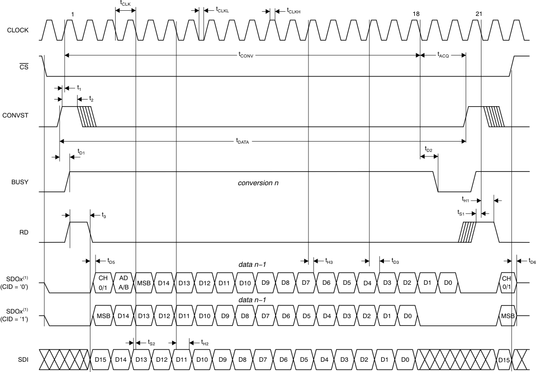
1. The ADS7263 and ADS7223 output data with the MSB located as the ADS8363 and the last 2 or 4 bits are '0'.
Figure 1. Detailed Timing Diagram: Half-Clock Mode (ADS8361-Compatible)
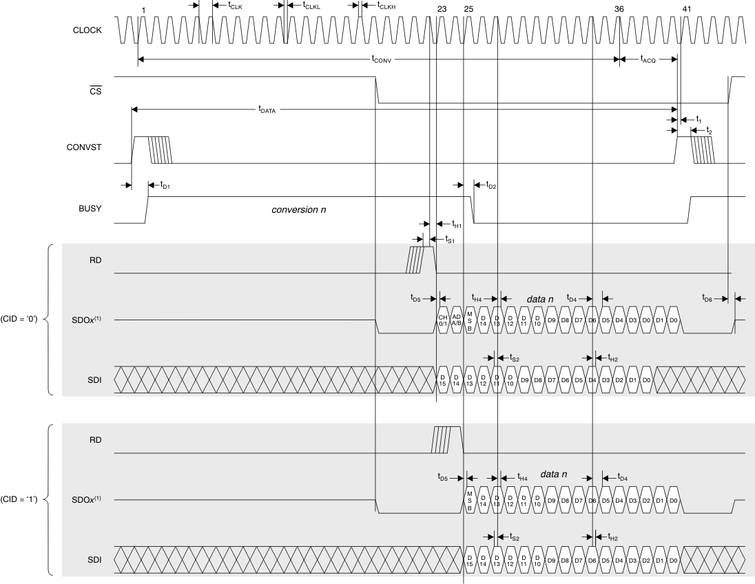
1. The ADS7263 and ADS7223 output data with the MSB located as the ADS8363 and the last 2 or 4 bits are '0'.
Figure 2. Detailed Timing Diagram: Full-Clock Mode
7.10 Typical Characteristics
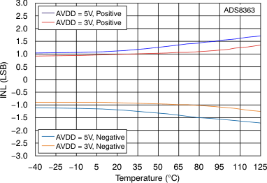
at TA = +25°C, AVDD = 5 V, DVDD = 3.3 V, VREF = 2.5 V (internal), and fDATA = 1 MSPS (unless otherwise noted)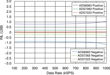
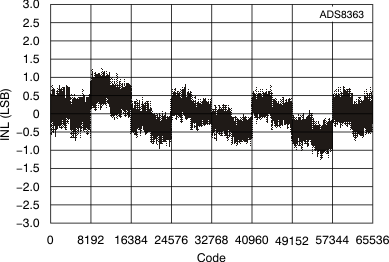
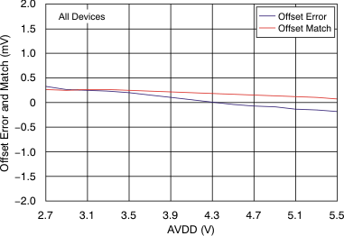
Analog Supply Voltage
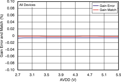
Analog Supply Voltage
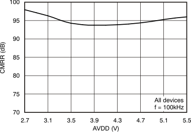
Analog Supply Voltage
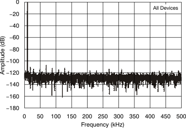
(4096 Point FFT; fIN = 10 kHz)
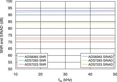
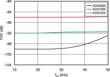
Input Signal Frequency
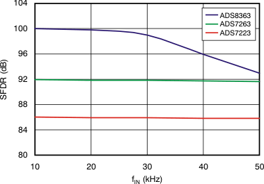
Input Signal Frequency
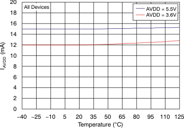
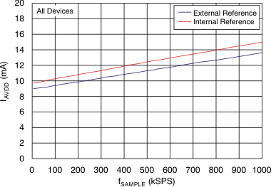
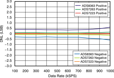
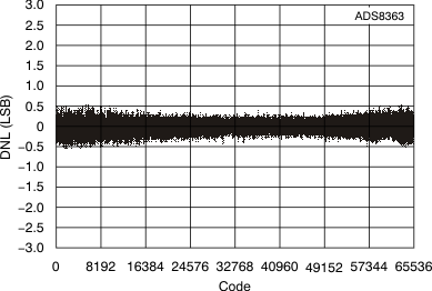
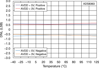
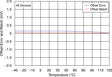
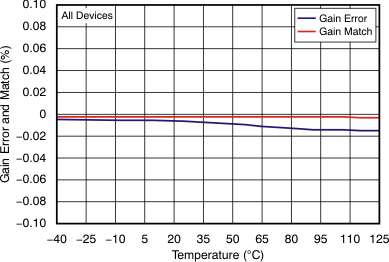
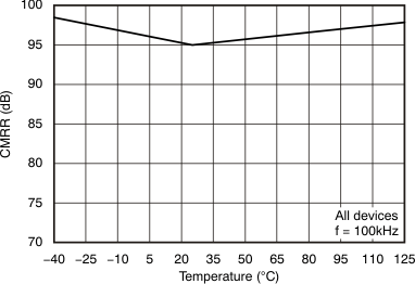
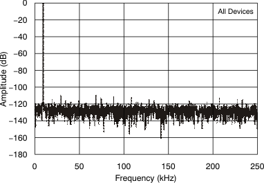
(4096 Point FFT; fIN = 10 kHz, fSAMPLE = 0.5 MSPS)
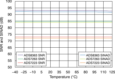
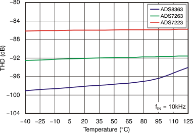
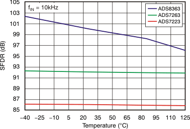
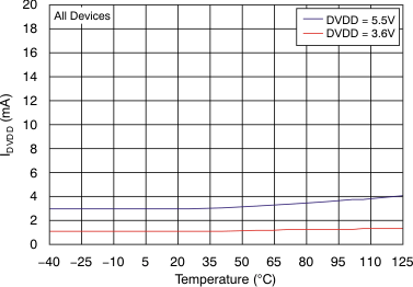
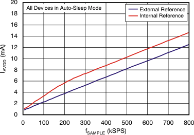
(Auto-Sleep Mode)