SBAS523D October 2010 – September 2017 ADS7223 , ADS7263 , ADS8363
PRODUCTION DATA.
- 1 Features
- 2 Applications
- 3 Description
- 4 Revision History
- 5 Device Comparison Table
- 6 Pin Configuration and Functions
-
7 Specifications
- 7.1 Absolute Maximum Ratings
- 7.2 ESD Ratings
- 7.3 Recommended Operating Conditions
- 7.4 Thermal Information
- 7.5 Electrical Characteristics: General
- 7.6 Electrical Characteristics: ADS8363
- 7.7 Electrical Characteristics: ADS7263
- 7.8 Electrical Characteristics: ADS7223
- 7.9 Switching Characteristics
- 7.10 Typical Characteristics
- 8 Detailed Description
- 9 Application and Implementation
- 10Power Supply Recommendations
- 11Layout
- 12Device and Documentation Support
- 13Mechanical, Packaging, and Orderable Information
9 Application and Implementation
NOTE
Information in the following applications sections is not part of the TI component specification, and TI does not warrant its accuracy or completeness. TI’s customers are responsible for determining suitability of components for their purposes. Customers should validate and test their design implementation to confirm system functionality.
9.1 Application Information
9.1.1 ADS8361 Compatibility
This section describes the differences between the ADS8361 and the ADS8363, ADS7263, and ADS7223 family of devices in default mode without changing the internal register settings (that are not available on the ADS8361).
9.1.1.1 Pinout
The ADS8363, ADS7263, and ADS7223 family is pin-compatible to ADS8361IRHB. However, there are some differences that must be considered when migrating from an ADS8361-based design, as summarized in Table 10.
Table 10. Pinout Differences Between the ADS8363, ADS7263, and ADS7223 and the ADS8361
| PIN NO. | PIN NAME | IMPACT | |
|---|---|---|---|
| ADS8361 | ADS8363, ADS7263, and ADS7223 | ||
| 9 | REFIN | REFIO1 | If external reference is used, see the Internal Reference section for details. If internal reference is used, REFIO1 must be enabled using the RPD bit in the DAC1 register. |
| 10 | REFOUT | REFIO2 | Because REFIO2 is disabled by default, no adjustment is required. |
| 11 | NC | RGND | If external reference is used, no changes required. If REFIO1 is enabled, this pin must be tied to the analog ground plane with a dedicated via. Furthermore, a 22-µF ceramic capacitor must be used between this pin and pin 9. |
| 18 | A0 | SDI | See the SDI versus A0 section for details. |
| 29 | NC | AVDD | This pin must be connected to the analog supply and decoupled with a 1-µF capacitor to ensure proper functionality of the ADS8363, ADS7263, and ADS7223 family. |
| 30 | NC | AGND | This pin must be connected to the analog ground plane to ensure proper functionality of the ADS8363, ADS7263, and ADS7223 family. |
| 31 | NC | CMA | In default mode of the ADS8363 family; no changes required. |
| 32 | NC | CMB | In default mode of the ADS8363 family; no changes required. |
9.1.1.2 SDI versus A0
Pin 18 (SDI) of the ADS8363, ADS7263, and ADS7223 is used to update the internal registers, whereas on the ADS8361, pin 18 (A0) is used in conjunction with M0 to select the input channel.
If, in an existing design, the ADS8361 is used in two-channel mode (M0 = '0') and the status of the A0 pin is unchanged within the first four clock cycles after issuing a conversion start (rising edge of CONVST), the ADS8363, ADS7263, and ADS7223 act similarly to the ADS8361 and convert either channels CHx0 (if SDI is held low during the entire period) or channels CHx1 (if SDI is held high during the entire period). Figure 34 illustrates the behavior of the ADS8363, ADS7263, and ADS7223 in such a situation.
The ADS8363, ADS7263, and ADS7223 can be also be used to replace the ADS8361 when run in four-channel mode (M0 = '1'). In this case, the A0 pin is held static (high or low), which is also required in for the SDI pin to prevent accidental update of the SDI register.
In both cases described previously, the additional features of the ADS8363, ADS7263, and ADS7223 (pseudo-differential input mode, programmable reference voltage output, and the various power-down modes) cannot be accessed, but the hardware and software remain backward-compatible to the ADS8361.
9.1.1.3 Internal Reference
The internal reference of the ADS8361 delivers 2.5 V (typ) after power up, and the reference output of the ADS8363, ADS7263, and ADS7223 is powered down by default. In this case, the unbuffered reference input has a code-dependent input impedance, and the ADS8361 offers a high-impedance (buffered) reference input. If an existing ADS8361-based design uses the internal reference of the device and relies on an external resistor divider to adjust the input voltage range of the ADC, migration to the ADS8363 family requires one of the following conditions:
- A software change to setup internal reference DAC1 properly through SDI when removing the external resistors; or
- An additional external buffer between the resistor divider and the required 22 µF (min) capacitor on the REFIO1 input.
In the latter case, when the capacitor stabilizes the reference voltage during the entire conversion, the buffer must recharge the capacitor by providing an average current only; thus, the required minimum bandwidth of the buffer can be calculated using Equation 4:

The buffer must also be capable of driving the 22-µF load when maintaining stability.
9.1.1.4 Timing
In half-clock mode (default), the ADS8363, ADS7263, and ADS7223 family of devices provides the conversion delay after completion of the conversion (see Figure 1), and the ADS8361 offers the conversion result during the conversion process.
9.1.1.5 RD
The ADS8363, ADS7263, and ADS7223 output the first bit with the falling edge of the RD input. The ADS8361 starts the data transfer with the first falling edge of the clock if RD is high.
If the ADS8363, ADS7263, and ADS7223 operate with half-clock timing in modes II and IV, the RD input must not be held high longer than one clock cycle to ensure proper function of the data output SDOA.
9.1.2 Minimum Configuration Example
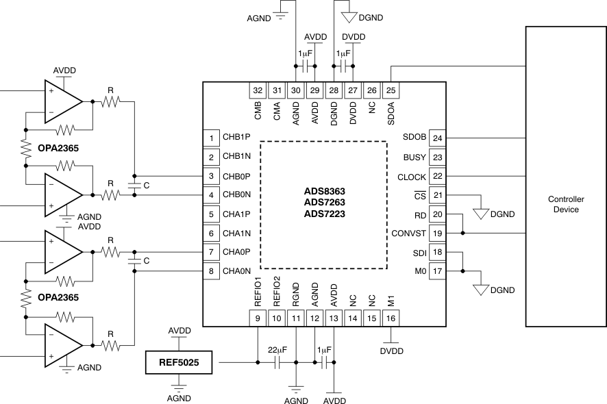
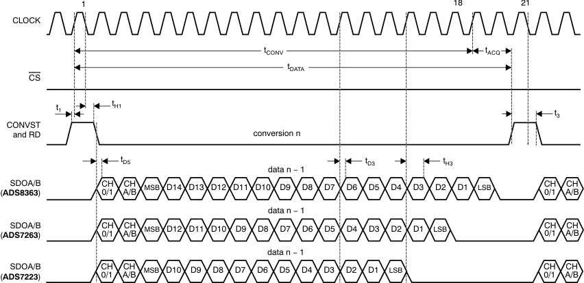
An example of a minimum configuration for the ADS8363, ADS7263, and ADS7223 is illustrated in Figure 47. In this case, the device is used in dual-channel, fully-differential input mode with a four-wire digital interface connected to the controller device and with default settings of the device after power up. Because the internal reference is disabled at power up (to prevent driving against an external reference if used), an external reference source is shown in this example. To allow the use of the internal reference, the SDI input must be connected to the controller, allowing access to the REFDAC registers. The corresponding timing diagram including the timing requirements are described in Figure 48 and the Timing Characteristics table.
The input signal for the amplifiers must fulfill the common-mode voltage requirements of the device in this configuration. The actual values of the resistors and capacitors depend on the bandwidth and performance requirements of the application.
Those values can be calculated using Equation 5:

where
- n = 16 as the resolution of the ADS8363 (n = 14 for ADS7263, n = 12 for ADS7223)
As a good trade-off between required minimum driver bandwidth and the capacitor value, a capacitor value of at least 1 nF is recommended.
Keeping the acquisition time in mind, the resistor value can be calculated as shown in Equation 6 for each of the series resistors:

where
- n = the device resolution
 Figure 47. Four-Wire Application Configuration
