SLAS600C May 2008 – December 2016 ADS8319
PRODUCTION DATA.
- 1 Features
- 2 Applications
- 3 Description
- 4 Revision History
- 5 Device Comparison Table
- 6 Pin Configuration and Functions
- 7 Specifications
- 8 Detailed Description
- 9 Application and Implementation
- 10Power Supply Recommendations
- 11Layout
- 12Device and Documentation Support
- 13Mechanical, Packaging, and Orderable Information
封装选项
机械数据 (封装 | 引脚)
散热焊盘机械数据 (封装 | 引脚)
- DRC|10
订购信息
9 Application and Implementation
NOTE
Information in the following applications sections is not part of the TI component specification, and TI does not warrant its accuracy or completeness. TI’s customers are responsible for determining suitability of components for their purposes. Customers should validate and test their design implementation to confirm system functionality.
9.1 Application Information
To maximize the performance of data acquisition (DAQ) system based on a high precision, successive approximation register (SAR), analog-to-digital converter (ADC), the input driver and the reference driver circuits must be designed properly and must be optimized. This section details some general principles for designing these circuits, followed by an application circuit designed using the ADS8319.
9.2 Typical Application
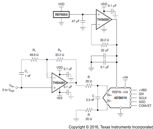
This section describes a typical application circuit using the ADS8319. For simplicity, the power-supply circuit and decoupling capacitors are not shown in this circuit diagram.
 Figure 61. Unipolar Single-Ended Input DAQ System
9.2.1 Design Requirements
This application circuit for ADS8319 (as shown in Figure 61) is designed to achieve the key specific performance at a maximum specified throughput of 500 kSPS below:
- SNR > 92 dB
- THD < 111 dB
- Lower power consumption
9.2.2 Detailed Design Procedure
The reference driver circuit illustrated in Figure 61 generates 5-V DC using a single supply. This circuit is suitable to drive the reference at sampling rates of up to 500 kSPS. To keep the noise low and maximize the dynamic range, a high-precision, low-noise REF5050 voltage reference is used in this DAQ system
For the input driver, the distortion of the amplifier must be at least 10 dB less than the ADC distortion. The low-power feature of ADS8319 makes it suitable for a low power DAQ system design. The THS4281 (low-power, high-speed voltage-feedback operational amplifier) is a perfect choice for input and reference driver of ADS8319 to offer a very low quiescent current (less than 1 mA) across the supply and temperature and drive large capacitive loads that regulate the voltage at the input and reference input pins of the ADC, its high bandwidth (40 MHz, specified at gain of 2) can make the signal settle quickly, also the Rail-to-Rail input and output feature can maximize the dynamic range of ADC as a driver.
Finally, the components of the balanced low-pass RC filter are chosen such that the noise from the front-end circuit is kept low without adding distortion to the input signal.
For detailed design information, see Low Power Input and Reference Driver Circuit for Reference Driver Circuit for ADS8318 and ADS8319 (SBOA118).
9.2.3 Application Curves
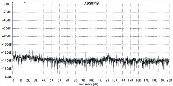
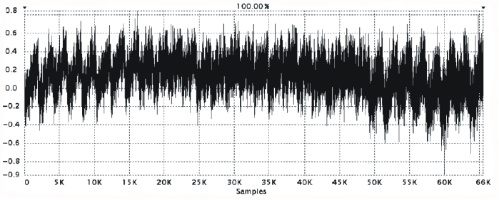
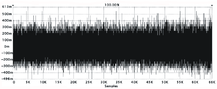
This section presents the performance results obtained on several devices for the driver and shown in Figure 62 through Figure 64.
Table 2 summarizes the test results obtained for the circuit shown in Figure 61.
Table 2. Performance Results for ADS8319 DAQ System
| PARAMETER | ADS8319 DATA SHEET LIMITS | ADS8319 WITH THS4031 | ADS8319 WITH THS4281 |
|---|---|---|---|
| DNLMAX | < 1.5 | 0.54 | 0.65 |
| DNLMin | > –1 | –0.5 | –0.53 |
| INLMAX | < 2.5 | 0.62 | 0.83 |
| INLMIN | > –2.5 | –0.95 | –0.65 |
| SNR | >92 dB | 93.9 dB | 92.5 dB |
| THD | –111 (typical) | –113 dB | –113 dB |
| SFDR | 113 (typical) | 115 dB | 115 dB |
| SINAD | 93.8 (typical) | 93.8 dB | 92.4 dB |
| Circuit power consumption | — | 205.6 mW | 38.44 mW |

| 1.9-kHz input signal | |
 Figure 64. Typical INL Graph
