ZHCSJ06B November 2017 – September 2022 ADS7142-Q1
PRODUCTION DATA
- 1 特性
- 2 应用
- 3 说明
- 4 Revision History
- 5 Pin Configuration and Functions
-
6 Specifications
- 6.1 Absolute Maximum Ratings
- 6.2 ESD Ratings
- 6.3 Recommended Operating Conditions
- 6.4 Thermal Information
- 6.5 Electrical Characteristics: All Modes
- 6.6 Electrical Characteristics: Manual Mode
- 6.7 Electrical Characteristics: Autonomous Modes
- 6.8 Electrical Characteristics: High Precision Mode
- 6.9 Timing Requirements
- 6.10 Switching Characteristics
- 6.11 Timing Diagrams
- 6.12 Typical Characteristics: All Modes
- 6.13 Typical Characteristics: Manual Mode
- 6.14 Typical Characteristics: Autonomous Modes
- 6.15 Typical Characteristics: High-Precision Mode
-
7 Detailed Description
- 7.1 Overview
- 7.2 Functional Block Diagram
- 7.3 Feature Description
- 7.4 Device Functional Modes
- 7.5 Programming
- 7.6 Register Map
- 8 Application and Implementation
- 9 Device and Documentation Support
- 10Mechanical, Packaging, and Orderable Information
7.3.1 Analog Input and Multiplexer
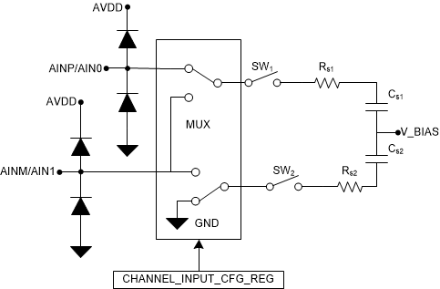
Figure 7-1 shows a small-signal equivalent circuit for the analog input pins. The device includes a two-channel analog multiplexer with each input pin having ESD protection diodes to AVDD and GND. The sampling switches are represented by ideal switches SW1 and SW2 in series with resistors Rs1 and Rs2 (typically 150 Ω). The sampling capacitors, Cs1 and Cs2, are typically 15 pF. The multiplexer configuration is set by the CH_INPUT_CFG register.
During acquisition, switches SW1 and SW2 are closed to allow the input signal to charge the internal sampling capacitors.
During conversion, switches SW1 and SW2 are opened to disconnect the input signal from the sampling capacitors.
The analog inputs of the device are optimized to be driven by a high-impedance source (up to 100 kΩ) in autonomous modes or in high precision mode with a low-power oscillator. When using the high-speed oscillator, drive the analog inputs of the ADC with an external amplifier in autonomous modes or in high precision mode. Figure 6-29 and Figure 6-30 provide the analog input current for CH0 and CH1 of the device.
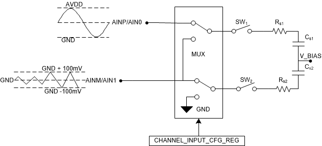
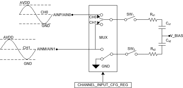
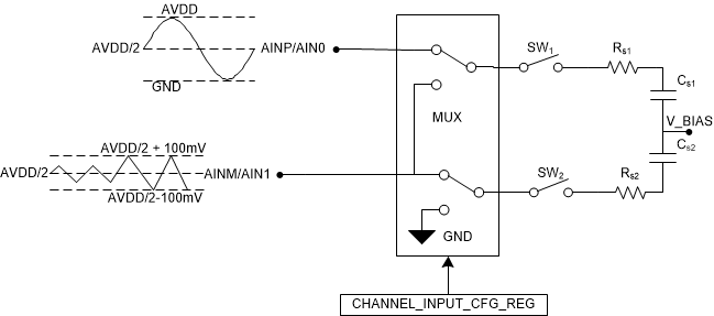
Figure 7-2, Figure 7-3, and Figure 7-4 provide a simplified circuit for analog input for input configurations described in the Section 7.3.1.1, Section 7.3.1.2, and Section 7.3.1.3 sections, respectively. The analog multiplexer supports following input configurations (set by writing into the CH_INPUT_CFG register).
 Figure 7-1 Equivalent Circuit for Analog Input
 Figure 7-3 Single-Channel, Single-Ended Configuration With Remote Ground Sensing
 Figure 7-2 Two-Channel, Single-Ended Configuration
 Figure 7-4 Single-Channel, Pseudo-Differential Configuration