ZHCSAK5C December 2012 – December 2015 ADS42B49
PRODUCTION DATA.
- 1 特性
- 2 应用
- 3 说明
- 4 修订历史记录
- 5 Description (continued)
- 6 ADS424x and ADS422x Family Comparison
- 7 Pin Configuration and Functions
-
8 Specifications
- 8.1 Absolute Maximum Ratings
- 8.2 ESD Ratings
- 8.3 Recommended Operating Conditions
- 8.4 Thermal Information
- 8.5 Electrical Characteristics: ADS42B49 (250 MSPS)
- 8.6 Electrical Characteristics: General
- 8.7 Digital Characteristics
- 8.8 Timing Requirements: LVDS and CMOS Modes
- 8.9 Serial Interface Timing Characteristics
- 8.10 Reset Timing (Only When Serial Interface is Used)
- 8.11 LVDS Timings at Lower Sampling Frequencies
- 8.12 CMOS Timings at Lower Sampling Frequencies
- 8.13 Typical Characteristics
- 9 Parameter Measurement Information
- 10Detailed Description
- 11Application and Implementation
- 12Power Supply Recommendations
- 13Layout
- 14器件和文档支持
- 15机械、封装和可订购信息
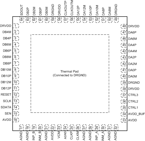
7 Pin Configuration and Functions
RGC Package(1)
64-Pin VQFN With Exposed Thermal Pad
LVDS Mode - Top View

1. The thermal pad is connected to DRGND.
Pin Functions - LVDS Mode
| PIN | I/O | DESCRIPTION | |
|---|---|---|---|
| NAME | NO. | ||
| AGND | 17, 18, 21, 24, 27, 28, 31, 32 | Input | Analog ground |
| AVDD | 16, 22, 33 | Input | Analog power supply |
| AVDD_BUF | 34 | Input | Analog buffer supply |
| CLKM | 26 | Input | Differential clock negative input |
| CLKP | 25 | Input | Differential clock positive input |
| CLKOUTM | 56 | Output | Differential output clock, complement |
| CLKOUTP | 57 | Output | Differential output clock, true |
| CTRL1 | 35 | Input | Digital control input pins. Together, these pins control the various power-down modes. |
| CTRL2 | 36 | Input | Digital control input pins. Together, these pins control the various power-down modes. |
| CTRL3 | 37 | Input | Digital control input pins. Together, these pins control the various power-down modes. |
| DA0P, DA0M | 41, 40 | Output | Channel A differential output data pair, D0 and D1 multiplexed |
| DA2P, DA2M | 43, 42 | Output | Channel A differential output data D2 and D3 multiplexed |
| DA4P, DA4M | 45, 44 | Output | Channel A differential output data D4 and D5 multiplexed |
| DA6P, DA6M | 47, 46 | Output | Channel A differential output data D6 and D7 multiplexed |
| DA8P, DA8M | 51, 50 | Output | Channel A differential output data D8 and D9 multiplexed |
| DA10P, DA10M | 53, 52 | Output | Channel A differential output data D10 and D11 multiplexed |
| DA12P, DA12M | 55, 54 | Output | Channel A differential output data D12 and D13 multiplexed |
| DB0P, DB0M | 61, 60 | Output | Channel B differential output data pair, D0 and D1 multiplexed |
| DB2P, DB2M | 63, 62 | Output | Channel B differential output data D2 and D3 multiplexed |
| DB4P, DB4M | 3, 2 | Output | Channel B differential output data D4 and D5 multiplexed |
| DB6P, DB6M | 5, 4 | Output | Channel B differential output data D6 and D7 multiplexed |
| DB8P, DB8M | 7, 6 | Output | Channel B differential output data D8 and D9 multiplexed |
| DB10P, DB10M | 9, 8 | Output | Channel B differential output data D10 and D11 multiplexed |
| DB12P, DB12M | 11, 10 | Output | Channel B differential output data D12 and D13 multiplexed |
| DRGND | 39, 49, 59, PAD | Input | Output buffer ground, should be shorted on-board to analog ground. |
| DRVDD | 1, 38, 48, 58 | Input | Output buffer supply |
| INM_A | 30 | Input | Differential analog negative input, channel A |
| INP_A | 29 | Input | Differential analog positive input, channel A |
| INM_B | 20 | Input | Differential analog negative input, channel B |
| INP_B | 19 | Input | Differential analog positive input, channel B |
| RESET | 12 | Input | Serial interface RESET input. When using the serial interface mode, the internal registers must be initialized through a hardware RESET by applying a high pulse on this pin or by using the software reset option; refer to the Serial Interface Configuration section. In parallel interface mode, the RESET pin must be permanently tied high. SCLK and SEN are used as parallel control pins in this mode. This pin has an internal 150-kΩ pull-down resistor. |
| SCLK | 13 | Input | This pin functions as a serial interface clock input when RESET is low. SCLK controls the low-speed mode selection when RESET is tied high; see Table 6 for detailed information. This pin has an internal 150-kΩ pull-down resistor. |
| SDATA | 14 | Input | Serial interface data input; this pin has an internal 150-kΩ pull-down resistor. |
| SDOUT | 64 | Output | This pin functions as a serial interface register readout when the READOUT bit is enabled. When READOUT = 0, this pin is in high-impedance state. |
| SEN | 15 | Input | This pin functions as a serial interface enable input when RESET is low. SEN controls the output interface and data format selection when RESET is tied high; see Table 7 for detailed information. This pin has an internal 150-kΩ pull-up resistor to AVDD. |
| VCM | 23 | Output | This pin outputs the common-mode voltage (1.9 V) that can be used externally to bias the analog input pins |
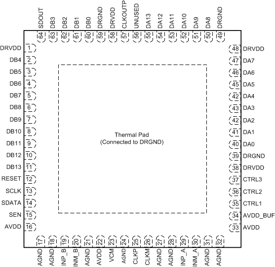
RGC Package(2)
64-Pin VQFN With Exposed Thermal Pad
CMOS Mode - Top View

1. The thermal pad is connected to DRGND.
Pin Functions - CMOS Mode
| PIN | I/O | DESCRIPTION | |
|---|---|---|---|
| NAME | NO. | ||
| AGND | 17, 18, 21, 24, 27, 28, 31, 32 | Input | Analog ground |
| AVDD | 16, 22, 33 | Input | Analog power supply |
| AVDD_BUF | 34 | Input | Analog buffer supply |
| CLKM | 26 | Input | Differential clock negative input |
| CLKP | 25 | Input | Differential clock positive input |
| CLKOUT | 57 | Output | CMOS output clock |
| CTRL1 | 35 | Input | Digital control input pins. Together, these pins control various power-down modes. |
| CTRL2 | 36 | Input | Digital control input pins. Together, these pins control various power-down modes. |
| CTRL3 | 37 | Input | Digital control input pins. Together, these pins control various power-down modes. |
| DA0 to DA13 | 40, 41, 42, 43, 44, 45, 46, 47, 50, 51, 52, 53, 54 ,55 | Output | Channel A ADC output data bits, CMOS levels |
| DB0 to DB13 | 60, 61, 62, 63, 2, 3, 4, 5, 6, 7, 8, 9, 10, 11 | Output | Channel B ADC output data bits, CMOS levels |
| DRGND | 39, 49, 59, PAD | Input | Output buffer ground, should be shorted on-board to analog ground. |
| DRVDD | 1, 38, 48, 58 | Input | Output buffer supply |
| INM_A | 30 | Input | Differential analog negative input, channel A |
| INP_A | 29 | Input | Differential analog positive input, channel A |
| INM_B | 20 | Input | Differential analog negative input, channel B |
| INP_B | 19 | Input | Differential analog positive input, channel B |
| RESET | 12 | Input | Serial interface RESET input. When using the serial interface mode, the internal registers must be initialized through a hardware RESET by applying a high pulse on this pin or by using the software reset option; refer to the Serial Interface Configuration section. In parallel interface mode, the RESET pin must be permanently tied high. SDATA and SEN are used as parallel control pins in this mode. This pin has an internal 150-kΩ pull-down resistor. |
| SCLK | 13 | Input | This pin functions as a serial interface clock input when RESET is low. SCLK controls the low-speed mode when RESET is tied high; see Table 6 for detailed information. This pin has an internal 150-kΩ pull-down resistor. |
| SDATA | 14 | Input | Serial interface data input; this pin has an internal 150-kΩ pull-down resistor. |
| SDOUT | 64 | Output | This pin functions as a serial interface register readout when the READOUT bit is enabled. When READOUT = 0, this pin is in high-impedance state. |
| SEN | 15 | Input | This pin functions as a serial interface enable input when RESET is low. SEN controls the output interface and data format selection when RESET is tied high; see Table 7 for detailed information. This pin has an internal 150-kΩ pull-up resistor to AVDD. |
| UNUSED | 56 | — | This pin is not used in the CMOS interface |
| VCM | 23 | Output | This pin outputs the common-mode voltage (1.9 V) that can be used externally to bias the analog input pins |