ZHCSAK5C December 2012 – December 2015 ADS42B49
PRODUCTION DATA.
- 1 特性
- 2 应用
- 3 说明
- 4 修订历史记录
- 5 Description (continued)
- 6 ADS424x and ADS422x Family Comparison
- 7 Pin Configuration and Functions
-
8 Specifications
- 8.1 Absolute Maximum Ratings
- 8.2 ESD Ratings
- 8.3 Recommended Operating Conditions
- 8.4 Thermal Information
- 8.5 Electrical Characteristics: ADS42B49 (250 MSPS)
- 8.6 Electrical Characteristics: General
- 8.7 Digital Characteristics
- 8.8 Timing Requirements: LVDS and CMOS Modes
- 8.9 Serial Interface Timing Characteristics
- 8.10 Reset Timing (Only When Serial Interface is Used)
- 8.11 LVDS Timings at Lower Sampling Frequencies
- 8.12 CMOS Timings at Lower Sampling Frequencies
- 8.13 Typical Characteristics
- 9 Parameter Measurement Information
- 10Detailed Description
- 11Application and Implementation
- 12Power Supply Recommendations
- 13Layout
- 14器件和文档支持
- 15机械、封装和可订购信息
13 Layout
13.1 Layout Guidelines
13.1.1 Grounding
A single ground plane is sufficient to give good performance, provided the analog, digital, and clock sections of the board are cleanly partitioned. Download the ADS42xx_58C28EVM DesignPkg file from the ADS42B49EVM product folder on the TI website for details on layout and grounding.
13.1.2 Supply Decoupling
Because the ADS42B49 already includes internal decoupling, minimal external decoupling can be used without loss in performance. Decoupling capacitors can help filter external power-supply noise; thus, the optimum number of capacitors depends on the actual application. The decoupling capacitors should be placed very close to the converter supply pins.
13.1.3 Exposed Pad
In addition to providing a path for heat dissipation, the PowerPAD is also electrically connected internally to the digital ground. Thus, the exposed pad must be soldered to the ground plane for best thermal and electrical performance. For detailed information, see application notes QFN Layout Guidelines (SLOA122) and QFN/SON PCB Attachment (SLUA271).
13.1.4 Routing Analog Inputs
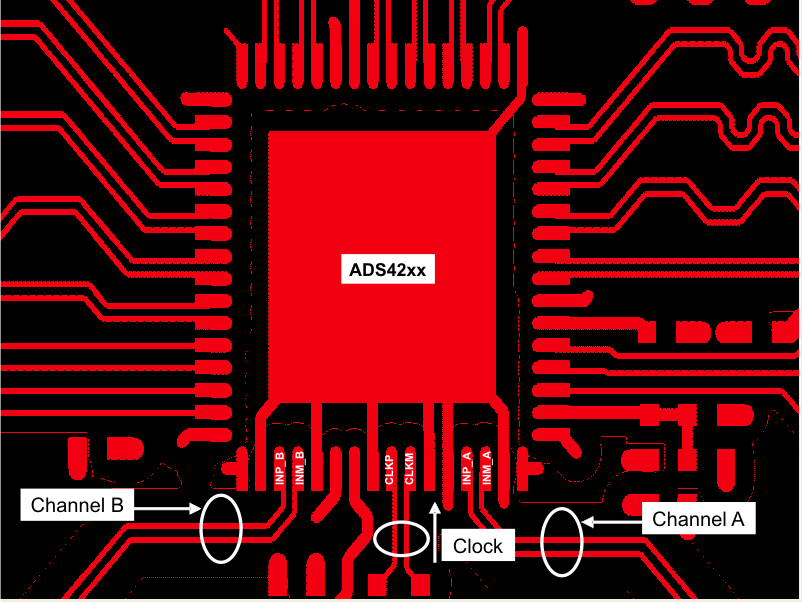
TI advises routing differential analog input pairs (INP_x and INM_x) close to each other. To minimize the possibility of coupling from a channel analog input to the sampling clock, the analog input pairs of both channels should be routed perpendicular to the sampling clock; see the ADS42Bx EVM User's Guide (SLAU477) for reference routing. Figure 65 shows a snapshot of the PCB layout from the ADS42xxEVM.
13.2 Layout Example
 Figure 65. ADS42xxEVM PCB Layout