ZHCSAK5C December 2012 – December 2015 ADS42B49
PRODUCTION DATA.
- 1 特性
- 2 应用
- 3 说明
- 4 修订历史记录
- 5 Description (continued)
- 6 ADS424x and ADS422x Family Comparison
- 7 Pin Configuration and Functions
-
8 Specifications
- 8.1 Absolute Maximum Ratings
- 8.2 ESD Ratings
- 8.3 Recommended Operating Conditions
- 8.4 Thermal Information
- 8.5 Electrical Characteristics: ADS42B49 (250 MSPS)
- 8.6 Electrical Characteristics: General
- 8.7 Digital Characteristics
- 8.8 Timing Requirements: LVDS and CMOS Modes
- 8.9 Serial Interface Timing Characteristics
- 8.10 Reset Timing (Only When Serial Interface is Used)
- 8.11 LVDS Timings at Lower Sampling Frequencies
- 8.12 CMOS Timings at Lower Sampling Frequencies
- 8.13 Typical Characteristics
- 9 Parameter Measurement Information
- 10Detailed Description
- 11Application and Implementation
- 12Power Supply Recommendations
- 13Layout
- 14器件和文档支持
- 15机械、封装和可订购信息
11 Application and Implementation
NOTE
Information in the following applications sections is not part of the TI component specification, and TI does not warrant its accuracy or completeness. TI’s customers are responsible for determining suitability of components for their purposes. Customers should validate and test their design implementation to confirm system functionality.
11.1 Application Information
The analog input pins have analog buffers (running off the AVDD_BUF supply) that internally drive the differential sampling circuit. As a result of the analog buffer, the input pins present high input impedance to the external driving source (10-kΩ dc resistance and 2.5-pF input capacitance). The buffer helps to isolate the external driving source from the switching currents of the sampling circuit. This buffering makes driving the buffered inputs easier than when compared to an ADC without the buffer.
The input common-mode is set internally using a 5-kΩ resistor from each input pin to VCM so the input signal can be ac-coupled to the pins. Each input pin (INP, INM) must swing symmetrically between VCM + 0.5 V and VCM – 0.5 V, resulting in a 2-V PP differential input swing.
The input sampling circuit has a high 3-dB bandwidth that extends up to 700 MHz (measured with 50-Ω source driving 50-Ω termination between INP and INM).
The dynamic offset of the first-stage sub-ADC limits the maximum analog input frequency to approximately 400 MHz (with 2-VPP amplitude) and to approximately 500 MHz (with 1.6-VPP amplitude) before the performance degrades. This offset is separate from the full-power analog bandwidth of 700 MHz, which is only an indicator of signal amplitude versus frequency.
11.1.1 Driving Circuit
Example driving circuit configuration is shown in Figure 53. Notice that the board circuitry is simplified compared to the non-buffered ADS4249.
To optimize even-harmonic performance at high input frequencies (greater than the first Nyquist), the use of back-to-back transformers is recommended, as shown in Figure 53. Note that the drive circuit is terminated by 50 Ω near the ADC side. The ac-coupling capacitors allow the analog inputs to self-bias around the required common-mode voltage.
 Figure 53. Drive Circuit for High Input Frequencies
The mismatch in the transformer parasitic capacitance (between the windings) results in degraded even-order harmonic performance. Connecting two identical RF transformers back-to-back helps minimize this mismatch and good performance is obtained for high-frequency input signals. An additional termination resistor pair may be required between the two transformers, as shown in Figure 53. The center point of this termination is connected to ground to improve the balance between the P (positive) and M (negative) sides. The values of the terminations between the transformers and on the secondary side must be chosen to obtain an effective 50 Ω (for a 50-Ω source impedance).
11.1.1.1 Drive Circuit Requirements
For optimum performance, the analog inputs must be driven differentially. This technique improves the common-mode noise immunity and even-order harmonic rejection. A small resistor (5 Ω to 10 Ω) in series with each input pin is recommended to damp out ringing caused by package parasitics.
Figure 54, Figure 55, and Figure 56 show the differential impedance (ZIN = RIN || CIN) at the ADC input pins. The presence of the analog input buffer results in an almost constant input capacitance up to 1 GHz.
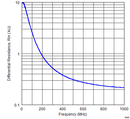 Figure 55. ADC Analog Input Resistance (RIN) Across Frequency
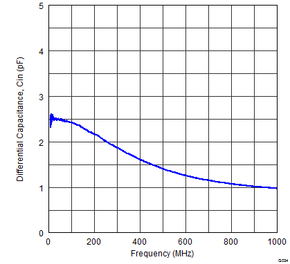 Figure 56. ADC Analog Input Capacitance (CIN) Across Frequency
11.1.2 Clock Input
The ADS42B49 clock inputs can be driven differentially (sine, LVPECL, or LVDS) or single-ended (LVCMOS), with little or no difference in performance between them. The common-mode voltage of the clock inputs is set to VCM using internal 5-kΩ resistors. This setting allows the use of transformer-coupled drive circuits for sine-wave clock or ac-coupling for LVPECL and LVDS clock sources are shown in Figure 57, Figure 58 and Figure 59. See Figure 60 details the internal clock buffer.
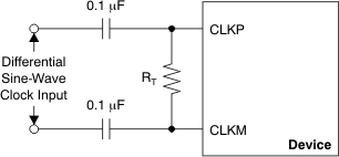
NOTE:
RT = termination resistor, if necessary.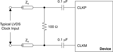 Figure 58. LVDS Clock Driving Circuit
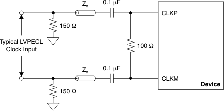 Figure 59. LVPECL Clock Driving Circuit
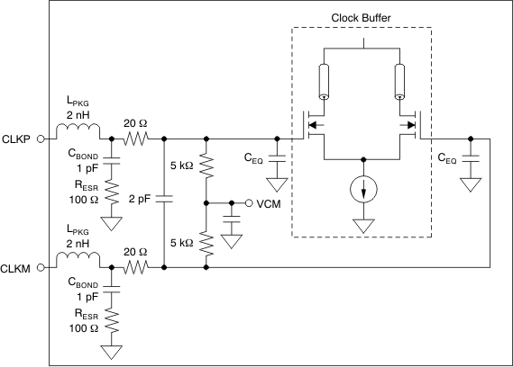
NOTE:
CEQ is 1 pF to 3 pF and is the equivalent input capacitance of the clock buffer.A single-ended CMOS clock can be ac-coupled to the CLKP input, with CLKM connected to ground with a 0.1-μF capacitor, as shown in Figure 61. For best performance, the clock inputs must be driven differentially, thereby reducing susceptibility to common-mode noise. For high input frequency sampling, TI recommends using a clock source with very low jitter. Band-pass filtering of the clock source can help reduce the effects of jitter. There is no change in performance with a non-50% duty cycle clock input.
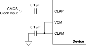 Figure 61. Single-Ended Clock Driving Circuit
11.2 Typical Application
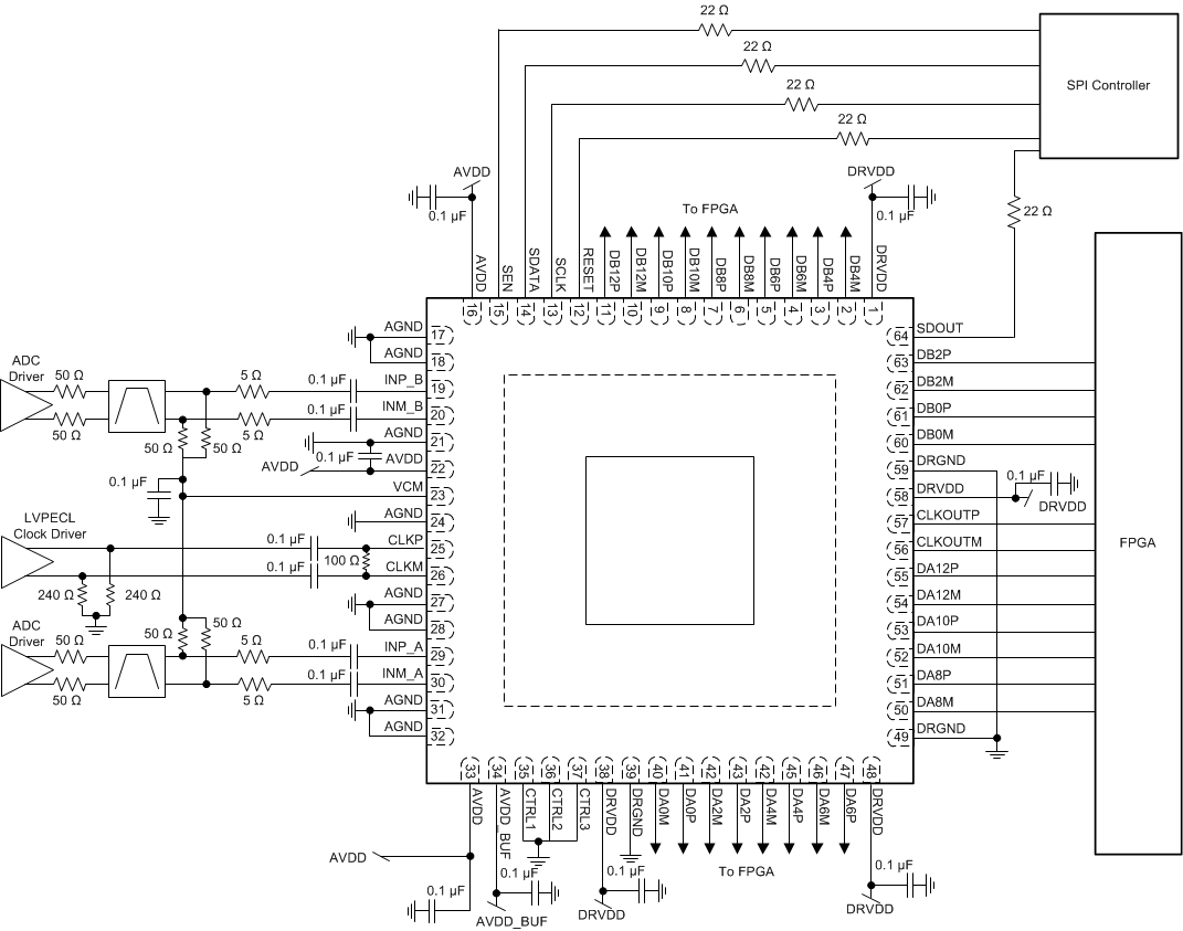 Figure 62. Example Schematic for ADS42B49
11.2.1 Design Requirements
Example design requirements are listed in Table 11 for the ADC portion of the signal chain. These do not necessary reflect the requirements of an actual system, but rather demonstrate why the ADS42B49 may be chosen for a system based on a set of requirements.
Table 11. Design Requirements for ADS42B49
| DESIGN PARAMETER | EXAMPLE DESIGN REQUIREMENT | ADS42B49 CAPABILITY |
|---|---|---|
| Sampling rate | ≥ 200 Msps to allow 125 MHz of unaliased bandwidth | Max sampling rate: 250 Msps |
| Input frequency | > 200 MHz to accommodate full 2nd nyquist zone | Large signal –3-dB bandwidth: 400-MHz operation |
| SNR | > 68 dBFS at –1 dFBS, 170 MHz | 70.7 dBFS at –1 dBFS, 170 MHz (0-dB gain) |
| SFDR | > 80 dBc at –1 dFBS, 170 MHz | 85 dBc at –1 dBFS, 170 MHz (0-dB gain) |
| Input full scale voltage | 1.5 Vpp | 1.5 Vpp |
| Overload recovery time | < 3 clock cycles | 1 clock cycle |
| Digital interface | DDR LVDS | DDR LVDS |
| Power consumption | < 500 mW per channel | 425 mW per channel |
11.2.2 Detailed Design Procedure
11.2.2.1 Analog Input
The analog input of the ADS42B49 is typically driven by a fully-differential amplifier. The amplifier must have sufficient bandwidth for the frequencies of interest. The noise and distortion performance of the amplifier affects the combined performance of the ADC and amplifier. The amplifier is often AC coupled to the ADC to allow both the amplifier and ADC to operate at the optimal common-mode voltages. The user can DC couple the amplifier to the ADC if required. An alternate approach is to drive the ADC using transformers. DC coupling cannot be used with the transformer approach.
11.2.2.2 Clock Driver
The ADS42B49 should be driven by a high performance clock driver, such as a clock jitter cleaner. The clock must have low noise to maintain optimal performance. LVPECL is the most common clocking interface, but LVDS and LVCMOS can also be used. Do not drive the clock input from an FPGA, unless the noise degradation can be tolerated, such as for input signals near DC where the clock noise impact is minimal.
11.2.2.3 Digital Interface
The ADS42B49 supports both LVDS and CMOS interfaces. The LVDS interface should be used for best performance when operating at maximum sampling rate. The LVDS outputs can be connected directly to the FPGA without any additional components. When using CMOS outputs, resistors should be placed in series with the outputs to reduce the output current spikes and limit the performance degradation. The resistors should be large enough to limit current spikes, but not so large as to significantly distort the digital output waveform. An external CMOS buffer should be used when driving distances greater than a few inches, to reduce ground bounce within the ADC.

