ZHCSEJ3B June 2015 – April 2020 ADS131E08S
PRODUCTION DATA.
- 1 特性
- 2 应用
- 3 说明
- 4 修订历史记录
- 5 Device Comparison
- 6 Pin Configuration and Functions
- 7 Specifications
- 8 Parameter Measurement Information
-
9 Detailed Description
- 9.1 Overview
- 9.2 Functional Block Diagram
- 9.3 Feature Description
- 9.4 Device Functional Modes
- 9.5
Programming
- 9.5.1 SPI Interface
- 9.5.2 Data Retrieval
- 9.5.3
SPI Command Definitions
- 9.5.3.1 WAKEUP: Exit STANDBY Mode
- 9.5.3.2 STANDBY: Enter STANDBY Mode
- 9.5.3.3 RESET: Reset Registers to Default Values
- 9.5.3.4 START: Start Conversions
- 9.5.3.5 STOP: Stop Conversions
- 9.5.3.6 OFFSETCAL: Channel Offset Calibration
- 9.5.3.7 RDATAC: Start Read Data Continuous Mode
- 9.5.3.8 SDATAC: Stop Read Data Continuous Mode
- 9.5.3.9 RDATA: Read Data
- 9.5.3.10 RREG: Read from Register
- 9.5.3.11 WREG: Write to Register
- 9.5.3.12 Sending Multibyte Commands
- 9.6
Register Map
- 9.6.1
Register Descriptions
- 9.6.1.1 ID: ID Control Register (Factory-Programmed, Read-Only) (address = 00h) [reset = D2h]
- 9.6.1.2 CONFIG1: Configuration Register 1 (address = 01h) [reset = 94h]
- 9.6.1.3 CONFIG2: Configuration Register 2 (address = 02h) [reset = 00h]
- 9.6.1.4 CONFIG3: Configuration Register 3 (address = 03h) [reset = E0h]
- 9.6.1.5 FAULT: Fault Detect Control Register (address = 04h) [reset = 00h]
- 9.6.1.6 CHnSET: Individual Channel Settings (address = 05h to 0Ch) [reset = 10h]
- 9.6.1.7 FAULT_STATP: Fault Detect Positive Input Status (address = 12h) [reset = 00h]
- 9.6.1.8 FAULT_STATN: Fault Detect Negative Input Status (address = 13h) [reset = 00h]
- 9.6.1.9 GPIO: General-Purpose IO Register (address = 14h) [reset = 0Fh]
- 9.6.1
Register Descriptions
- 10Application and Implementation
- 11Power Supply Recommendations
- 12Layout
- 13器件和文档支持
- 14机械、封装和可订购信息
11.1 Power-Up Timing
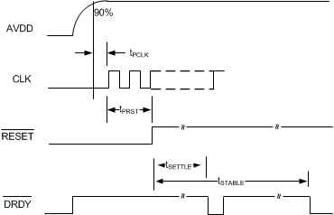
Settled data from the ADS131E08S are available within 3 ms of power-up if a strict timing sequence is followed. Before device power-up, all digital and analog inputs must be held low. Provide the master clock 50 µs after the analog and digital supplies reach 90% of their nominal values, shown as tPCLK in Figure 66. Pull the RESET pin high following the tPRST timing to bring the ADC digital filters out of a reset state and to begin the conversion process.
Settled data are available at the first DRDY falling edge, shown as tSETTLE in Figure 66. These data are from the settled digital filter; however, the first data set may not be a settled representation of the input because additional time is required for the reference and critical voltage nodes to settle to their final values. The tSTABLE timing adds the recommended wait time for settled data to be available at the ADC output. When the tSTABLE time has passed, the next DRDY falling edge indicates a valid conversion result of the input signal where both the digital filter and node voltages are settled.
 Figure 66. Power-Up Timing Diagram
 Table 22. Power-Up Sequence Timing
| MIN | TYP | MAX | UNIT | ||
|---|---|---|---|---|---|
| tPCLK | Delay time, first external CLK rising edge after AVDD reaches 90% | 50 | µs | ||
| Delay time, internal oscillator start-up after AVDD reaches 90% | 20 | ||||
| tPRST | Delay time, RESET rising edge after first CLK rising edge | 2 | tCLK | ||
| tSETTLE | Settling time, first settled data after RESET rising edge(1) | 2312 | tCLK | ||
| tSTABLE | Settling time, valid data after RESET rising edge | 2.2 | ms | ||
To deviate from the default register settings, write to the ADS131E08S registers after pulling the RESET pin high. Changes to any of the registers delay the tSETTLE start point until the register write is complete. If the data rate is changed following the RESET pin going high, the tSETTLE timing takes on the settling characteristics of Table 5 relative to the completion of the command.