ZHCSGS4A August 2017 – February 2020 ADS114S06B , ADS114S08B
PRODUCTION DATA.
- 1 特性
- 2 应用
- 3 说明
- 4 修订历史记录
- 5 Device Comparison Table
- 6 Pin Configuration and Functions
- 7 Specifications
- 8 Parameter Measurement Information
-
9 Detailed Description
- 9.1 Overview
- 9.2 Functional Block Diagram
- 9.3
Feature Description
- 9.3.1 Multiplexer
- 9.3.2 Low-Noise Programmable Gain Amplifier
- 9.3.3 Voltage Reference
- 9.3.4 Clock Source
- 9.3.5 Delta-Sigma Modulator
- 9.3.6 Digital Filter
- 9.3.7 Excitation Current Sources (IDACs)
- 9.3.8 Bias Voltage Generation
- 9.3.9 System Monitor
- 9.3.10 Status Register
- 9.3.11 General-Purpose Inputs and Outputs (GPIOs)
- 9.3.12 Calibration
- 9.4 Device Functional Modes
- 9.5 Programming
- 9.6
Register Map
- 9.6.1 Configuration Registers
- 9.6.2
Register Descriptions
- 9.6.2.1 Device ID Register (address = 00h) [reset = xxh]
- 9.6.2.2 Device Status Register (address = 01h) [reset = 80h]
- 9.6.2.3 Input Multiplexer Register (address = 02h) [reset = 01h]
- 9.6.2.4 Gain Setting Register (address = 03h) [reset = 00h]
- 9.6.2.5 Data Rate Register (address = 04h) [reset = 14h]
- 9.6.2.6 Reference Control Register (address = 05h) [reset = 10h]
- 9.6.2.7 Excitation Current Register 1 (address = 06h) [reset = 00h]
- 9.6.2.8 Excitation Current Register 2 (address = 07h) [reset = FFh]
- 9.6.2.9 Sensor Biasing Register (address = 08h) [reset = 00h]
- 9.6.2.10 System Control Register (address = 09h) [reset = 10h]
- 9.6.2.11 Reserved Register (address = 0Ah) [reset = 00h]
- 9.6.2.12 Offset Calibration Register 1 (address = 0Bh) [reset = 00h]
- 9.6.2.13 Offset Calibration Register 2 (address = 0Ch) [reset = 00h]
- 9.6.2.14 Reserved Register (address = 0Dh) [reset = 00h]
- 9.6.2.15 Gain Calibration Register 1 (address = 0Eh) [reset = 00h]
- 9.6.2.16 Gain Calibration Register 2 (address = 0Fh) [reset = 40h]
- 9.6.2.17 GPIO Data Register (address = 10h) [reset = 00h]
- 9.6.2.18 GPIO Configuration Register (address = 11h) [reset = 00h]
- 10Application and Implementation
- 11Power Supply Recommendations
- 12Layout
- 13器件和文档支持
- 14机械、封装和可订购信息
封装选项
请参考 PDF 数据表获取器件具体的封装图。
机械数据 (封装 | 引脚)
- RHB|32
- PBS|32
散热焊盘机械数据 (封装 | 引脚)
订购信息
10.1.2 Analog Input Filtering
Analog input filtering serves two purposes: first, to limit the effect of aliasing during the sampling process and second, to reduce external noise from being a part of the measurement.
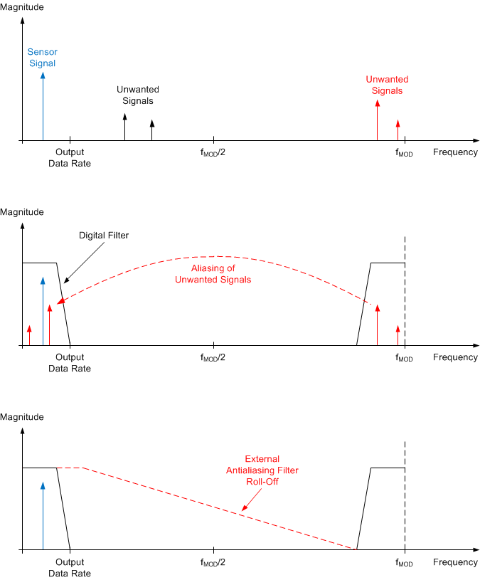
As with any sampled system, aliasing can occur if proper antialias filtering is not in place. Aliasing occurs when frequency components are present in the input signal that are higher than half the sampling frequency of the ADC (also known as the Nyquist frequency). These frequency components are folded back and show up in the actual frequency band of interest below half the sampling frequency. Inside a ΔΣ ADC, the input signal is oversampled at the modulator frequency, fMOD and not at the output data rate. Figure 95 shows that the filter response of the digital filter repeats at multiples of fMOD. Signals or noise up to a frequency where the filter response repeats are attenuated to a certain amount by the digital filter depending on the filter architecture. Any frequency components present in the input signal around the modulator frequency or multiples thereof are not attenuated and alias back into the band of interest, unless attenuated by an external analog filter.
 Figure 95. Effect of Aliasing
 Many sensor signals are inherently band limited; for example, the output of a thermocouple has a limited rate of change. In this case, the sensor signal does not alias back into the pass band when using a ΔΣ ADC. However, any noise pick-up along the sensor wiring or the application circuitry can potentially alias into the pass band. Power line-cycle frequency and harmonics are one common noise source. External noise can also be generated from electromagnetic interference (EMI) or radio frequency interference (RFI) sources, such as nearby motors and cellular phones. Another noise source typically exists on the printed circuit board (PCB) itself in the form of clocks and other digital signals. Analog input filtering helps remove unwanted signals from affecting the measurement result.
A first-order resistor-capacitor (RC) filter is (in most cases) sufficient to either eliminate aliasing, or to reduce the effect of aliasing to a level below the noise floor of the sensor. Ideally, any signal beyond fMOD / 2 is attenuated to a level below the noise floor of the ADC. The digital filter of the ADS114S0xB attenuates signals to a certain degree, as illustrated in the filter response plots in the Digital Filter section. In addition, noise components are usually smaller in magnitude than the actual sensor signal. Therefore, using a first-order RC filter with a cutoff frequency set at the output data rate or 10 times higher is generally a good starting point for a system design.
Internal to the device, prior to the PGA inputs, is an EMI filter; see Figure 43. The cutoff frequency of this filter is approximately 40 MHz and helps reject high-frequency interference.