ZHCSLJ1C July 2020 – December 2022 ADC3541 , ADC3542 , ADC3543
PRODUCTION DATA
- 1 特性
- 2 应用
- 3 说明
- 4 Revision History
- 5 Pin Configuration and Functions
-
6 Specifications
- 6.1 Absolute Maximum Ratings
- 6.2 ESD Ratings
- 6.3 Recommended Operating Conditions
- 6.4 Thermal Information
- 6.5 Electrical Characteristics - Power Consumption
- 6.6 Electrical Characteristics - DC Specifications
- 6.7 Electrical Characteristics - AC Specifications ADC3541
- 6.8 Electrical Characteristics - AC Specifications ADC3542
- 6.9 Electrical Characteristics - AC Specifications ADC3543
- 6.10 Timing Requirements
- 6.11 Typical Characteristics: ADC3541
- 6.12 Typical Characteristics: ADC3542
- 6.13 Typical Characteristics: ADC3543
- 7 Parameter Measurement Information
- 8 Detailed Description
- 9 Application Information Disclaimer
- 10Power Supply Recommendations
- 11Layout
- 12Device and Documentation Support
- 13Mechanical, Packaging, and Orderable Information
5 Pin Configuration and Functions
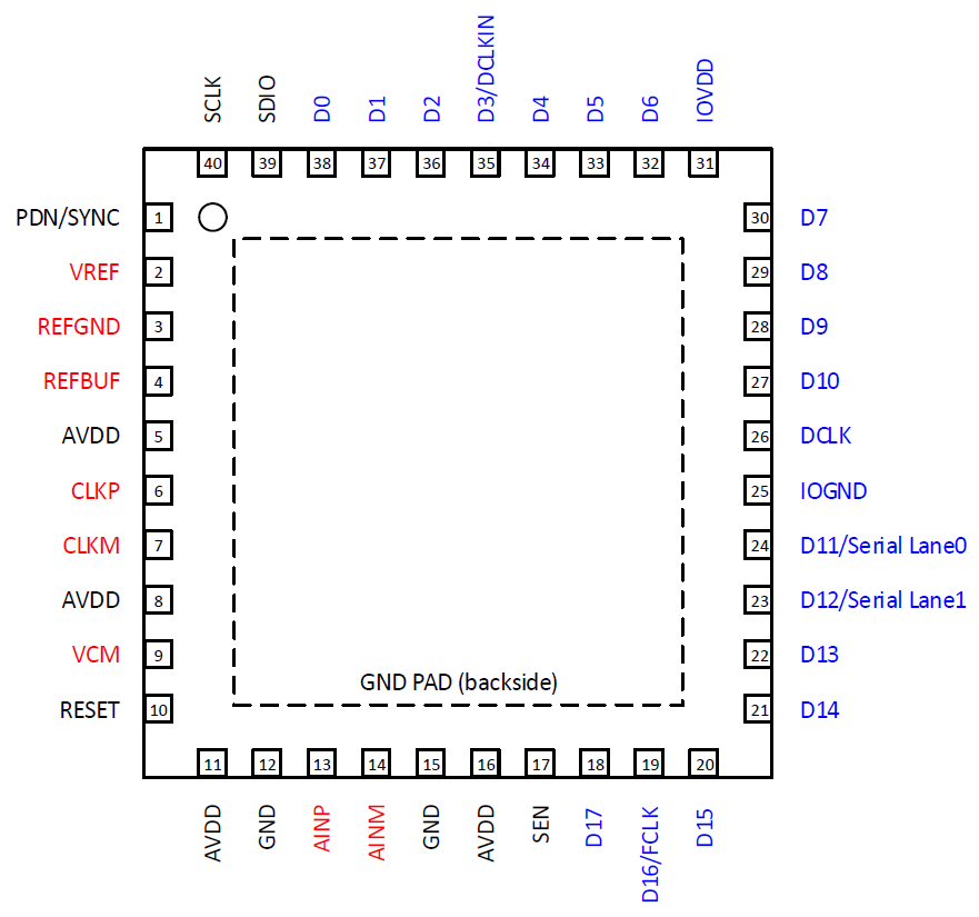
 Figure 5-1 RSB Package, 40-Pin WQFN
(Top View)
Table 5-1 Pin Descriptions
| PIN | I/O | DESCRIPTION | |
|---|---|---|---|
| NAME | NO. | ||
| INPUT/REFERENCE | |||
| AINM | 14 | I | Negative analog input |
| AINP | 13 | I | Positive analog input |
| REFBUF | 4 | I | 1.2-V external voltage reference input for use with internal reference buffer. Internal 100 kΩ pull-up resistor to AVDD. This pin is also used to configure default operating conditions. |
| REFGND | 3 | I | Reference ground input, 0 V |
| VCM | 9 | O | Common-mode voltage output for the analog inputs, 0.95 V |
| VREF | 2 | I | External voltage reference input, 1.6 V. |
| CLOCK | |||
| CLKM | 7 | I | Negative differential sampling clock input for the ADC |
| CLKP | 6 | I | Positive differential sampling clock input for the ADC |
| CONFIGURATION | |||
| PDN/SYNC | 1 | I | Power down, synchronization input. This pin can be configured via the SPI interface. Active high. This pin has an internal 21 kΩ pull-down resistor. |
| RESET | 10 | I | Hardware reset; active high. This pin has an internal 21 kΩ pull-down resistor. |
| SCLK | 40 | I | Serial interface clock input. This pin has an internal 21 kΩ pull-down resistor. |
| SDIO | 39 | I | Serial interface data input and output. This pin has an internal 21 kΩ pull-down resistor. |
| SEN | 17 | I | Serial interface enable. Active low. This pin has an internal 21 kΩ pull-up resistor to AVDD. |
| DIGITAL INTERFACE | |||
DCLK | 26 | O | CMOS output for data bit clock. |
| D0 | 38 | O | SDR CMOS output used with 18
bit output (configured via output bit formatter). This becomes the
LSB. When not used it can be left unconnected. See Section 8.3.5.4 and Section 8.3.5.5 on how to change the output resolution and output bit mapping. |
| D1 | 37 | O | SDR CMOS output used with 16 bit output (configured via output bit formatter). This becomes the LSB. When not used it can be left unconnected. |
| D2 | 36 | O | SDR CMOS output for data bit D0 (14 bit LSB). |
| D3/ DCLKIN | 35 | I/O | SDR CMOS output for data bit D1. Used as DCLKIN for serial CMOS output modes. |
| D4 | 34 | O | SDR CMOS output for data bit D2. |
| D5 | 33 | O | SDR CMOS output for data bit D3. |
| D6 | 32 | O | SDR CMOS output for data bit D4. |
| D7 | 30 | O | SDR CMOS output for data bit D5. |
| D8 | 29 | O | SDR CMOS output for data bit D6. |
| D9 | 28 | O | SDR CMOS output for data bit D7. |
| D10 | 27 | O | SDR CMOS output for data bit D8. |
| D11/ Serial Lane 0 | 24 | O | SDR CMOS output for data bit D9. DDR CMOS output for data bits D6/D13 (MSB). Lane 0 in serial CMOS output mode. |
| D12/ Serial Lane 1 | 23 | O | SDR CMOS output for data bit D10. DDR CMOS output for data bits D5/D12. Lane 1 in serial CMOS output mode. |
| D13 | 22 | O | SDR CMOS output for data bit D11. DDR CMOS output for data bits D4/D11. |
| D14 | 21 | O | SDR CMOS output for data bit D12. DDR CMOS output for data bits D3/D10. |
| D15 | 20 | O | CMOS output for data bit D13 (MSB). DDR CMOS output for data bits D2/D9. |
| D16/ FCLK | 19 | O | SDR CMOS output used with 16
bit output (configured via output bit formatter). This becomes the
MSB. When not used it can be left unconnected. DDR CMOS output for data bits D1/D8. Frame clock output in serial CMOS output mode. |
D17 | 18 | O | SDR CMOS output used with 18
bit output (configured via output bit formatter). This becomes the
MSB. When not used it can be left unconnected. DDR CMOS output for data bits D0/D7 (LSB). |
| POWER SUPPLY | |||
| AVDD | 5,8,11,16 | I | Analog 1.8-V power supply |
| GND | 12,15 | I | Ground, 0 V |
| IOGND | 25 | I | Ground, 0 V for digital interface |
| IOVDD | 31 | I | 1.8-V power supply for digital interface |
| PowerPAD™ | -- | -- | Connect to ground. |