SNAS466G February 2009 – December 2016 ADC10D1000QML-SP
PRODUCTION DATA.
- 1 Features
- 2 Applications
- 3 Description
- 4 Revision History
- 5 Pin Configuration and Functions
-
6 Specifications
- 6.1 Absolute Maximum Ratings
- 6.2 ESD Ratings
- 6.3 Recommended Operating Conditions
- 6.4 Thermal Information
- 6.5 Converter Electrical Characteristics: Static Converter Characteristics
- 6.6 Converter Electrical Characteristics: Dynamic Converter Characteristics
- 6.7 Converter Electrical Characteristics: Analog Input/Output and Reference Characteristics
- 6.8 Converter Electrical Characteristics: Channel-to-Channel Characteristics
- 6.9 Converter Electrical Characteristics: LVDS CLK Input Characteristics
- 6.10 Electrical Characteristics: AutoSync Feature
- 6.11 Converter Electrical Characteristics: Digital Control and Output Pin Characteristics
- 6.12 Converter Electrical Characteristics: Power Supply Characteristics (1:2 Demux Mode)
- 6.13 Converter Electrical Characteristics: AC Electrical Characteristics
- 6.14 Timing Requirements: Serial Port Interface
- 6.15 Timing Requirements: Calibration
- 6.16 Quality Conformance Inspection
- 6.17 Timing Diagrams
- 6.18 Typical Characteristics
-
7 Detailed Description
- 7.1 Overview
- 7.2 Functional Block Diagram
- 7.3 Feature Description
- 7.4
Device Functional Modes
- 7.4.1
Control Modes
- 7.4.1.1
Non-Extended Control Mode
- 7.4.1.1.1 Non-Demultiplexed Mode Pin (NDM)
- 7.4.1.1.2 Dual Data-Rate Phase Pin (DDRPh)
- 7.4.1.1.3 Calibration Pin (CAL)
- 7.4.1.1.4 Power-Down I-Channel Pin (PDI)
- 7.4.1.1.5 Power-Down Q-Channel Pin (PDQ)
- 7.4.1.1.6 Test Pattern Mode Pin (TPM)
- 7.4.1.1.7 Full-Scale Input Range Pin (FSR)
- 7.4.1.1.8 AC-DC-Coupled Mode Pin (VCMO)
- 7.4.1.1.9 LVDS Output Common-Mode Pin (VBG)
- 7.4.1.1
Non-Extended Control Mode
- 7.4.2 Extended Control Mode
- 7.4.1
Control Modes
- 7.5 Programming
- 7.6 Register Maps
- 8 Application and Implementation
- 9 Power Supply Recommendations
- 10Layout
- 11Device and Documentation Support
- 12Mechanical, Packaging, and Orderable Information
6 Specifications
6.1 Absolute Maximum Ratings
over operating free-air temperature range (unless otherwise noted)(1)(2)| MIN | MAX | UNIT | ||
|---|---|---|---|---|
| Supply voltage (VA, VTC, VDR, VE) | 2.2 | V | ||
| Supply difference – max(VA/TC/DR/E) – min(VA/TC/DR/E) | 0 | 100 | mV | |
| Voltage on any input pin (except VinI+, VinI–, VinQ+, VinQ–) | –0.15 | (VA + 0.15) | V | |
| VinI+, VinI–, VinQ+, VinQ– voltage(3) | –0.5 | 2.5 | V | |
| Input current at VinI+, VinI–, VinQ+, VinQ–(4) | 50 | mA | ||
| Ground difference – max(GNDTC/DR/E) – min(GNDTC/DR/E) | 0 | 100 | mV | |
| Input current at any pin(4) | ±50 | mA | ||
| Package power dissipation at TA ≤ 85°C(4) | 3.45 | W | ||
| Storage temperature, Tstg | –65 | 150 | °C | |
VA = VD = 2.2 V.
6.2 ESD Ratings
| VALUE | UNIT | |||
|---|---|---|---|---|
| V(ESD) | Electrostatic discharge | Human-body model (HBM), per ANSI/ESDA/JEDEC JS-001(1) | ±8000 | V |
| Charged-device model (CDM), per JEDEC specification JESD22-C101(2) | ±750 | |||
| Machine model | ±250 | |||
6.3 Recommended Operating Conditions
over operating free-air temperature range (unless otherwise noted)(1)| MIN | NOM | MAX | UNIT | ||
|---|---|---|---|---|---|
| Ambient temperature, TA | –55 | 125 | °C | ||
| Supply voltage (VA, VTC, VE) | 1.8 | 2 | V | ||
| Driver supply voltage (VDR) | 1.8 | VA | V | ||
| VinI+, VinI–, VinQ+, VinQ– voltage(2) | DC-coupled | –0.4 | 2.4 | V | |
| VinI+, VinI–, VinQ+, VinQ– differential voltage(3) | DC-coupled at 100% duty cycle | 1 | V | ||
| DC-coupled at 20% duty cycle | 2 | ||||
| DC-coupled at 10% duty cycle | 2.8 | ||||
| VinI+, VinI–, VinQ+, VinQ– current(2) | AC-coupled | –50 | 50 | mA | |
| VinI+, VinI–, VinQ+, VinQ– power | Maintaining common-mode voltage AC-coupled |
15.3 | dBm | ||
| Not maintaining common-mode voltage, AC-coupled |
17.1 | ||||
| Ground difference – max(GNDTC/DR/E) – min(GNDTC/DR/E) | 0 | V | |||
| CLK+, CLK– voltage | 0 | VA | V | ||
| Differential CLK amplitude | 0.4 | 2 | VP-P | ||
| VCMI common-mode input voltage | VCMO – 150 | VCMO + 150 | mV | ||
6.4 Thermal Information
| THERMAL METRIC(1)(2) | ADC10D1000QML-SP | UNIT | |
|---|---|---|---|
| NAA (CCGA) | |||
| 376 PINS | |||
| RθJA | Junction-to-ambient thermal resistance | 13.1 | °C/W |
| RθJC(top) | Junction-to-case (top) thermal resistance | 5.0 | °C/W |
| RθJB | Junction-to-board thermal resistance | 5.1 | °C/W |
| ψJT | Junction-to-top characterization parameter | 2.6 | °C/W |
| ψJB | Junction-to-board characterization parameter | 4.7 | °C/W |
6.5 Converter Electrical Characteristics: Static Converter Characteristics
The following specifications apply after calibration for VA = VDR = VTC = V = 1.9 V; I-channel and Q-channel AC-coupled, FSR pin = high; CL = 10 pF; differential AC-coupled sine wave input clock, fCLK = 1 GHz at 0.5 VP-P with 50% duty cycle; VBG = floating; non-extended control mode; Rext = Rtrim = 3300 Ω ±0.1%; analog signal source impedance = 100-Ω differential; 1:2 demultiplex non-DES mode; I channel and Q-channel; duty-cycle stabilizer on.(1)(2)(3)| PARAMETER | TEST CONDITIONS | SUB-GROUPS | MIN | TYP(4) | MAX | UNIT | ||
|---|---|---|---|---|---|---|---|---|
| INL | Integral non-linearity | DC-coupled, 1-MHz sine wave over-ranged | [1, 2, 3] | ±0.7 | ±1.4 | LSB | ||
| DNL | Differential non-linearity | DC-coupled, 1-MHz sine wave over-ranged | [1, 2, 3] | ±0.2 | ±0.5 | LSB | ||
| Resolution with no missing codes | [1, 2, 3] | 10 | bits | |||||
| VOFF | Offset error | –2.8 | LSB | |||||
| VOFF_ADJ | Input offset adjustment range | ±45 | mV | |||||
| PFSE | Positive full-scale error | See(5) | [1, 2, 3] | ±28 | mV | |||
| NFSE | Negative full-scale error | See(5) | [1, 2, 3] | ±28 | mV | |||
| Out-of-range output code | (VIN+) − (VIN−) > + full scale | [1, 2, 3] | 1023 | |||||
| (VIN+) − (VIN−) > – full scale | [1, 2, 3] | 0 | ||||||
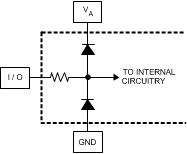
6.6 Converter Electrical Characteristics: Dynamic Converter Characteristics
The following specifications apply after calibration for VA = VDR = VTC = V = 1.9 V; I-channel and Q-channel AC-coupled, FSR pin = high; CL = 10 pF; differential AC-coupled sine wave input clock, fCLK = 1 GHz at 0.5 VP-P with 50% duty cycle; VBG = floating; non-extended control mode; Rext = Rtrim = 3300 Ω ±0.1%; analog signal source impedance = 100-Ω differential; 1:2 demultiplex non-DES mode; I channel and Q-channel; duty-cycle stabilizer on.(1)(2)(3)| PARAMETER | TEST CONDITIONS | SUB-GROUPS | MIN | TYP(4) | MAX | UNIT | |
|---|---|---|---|---|---|---|---|
| FPBW | Full-power bandwidth | Non-DES mode | 2.8 | GHz | |||
| DES mode | 1.3 | ||||||
| CER | Code error rate | 10–18 | Error/Sample | ||||
| Gain flatness | DC to 498 MHz | ±0.25 | dBFS | ||||
| DC to 1 GHz | ±0.5 | ||||||
| NPR | Noise power ratio | fc = 325 MHz, notch width = 25 MHz |
47.5 | dB | |||
| 1:2 DEMUX NON-DES MODE, EXTENDED CONTROL MODE, FM (14:0) = 7FFFh | |||||||
| ENOB | Effective number of bits | fIN = 248 MHz, VIN = –0.5 dBFS | [4, 5] | 8.4 | 9 | bits | |
| fIN = 248 MHz, VIN = –0.5 dBFS | [6] | 7.8 | 9 | ||||
| fIN = 498 MHz, VIN = –0.5 dBFS | [4, 5] | 8.2 | 8.9 | ||||
| fIN = 498 MHz, VIN = –0.5 dBFS, | [6] | 7.8 | 8.9 | ||||
| SINAD | Signal-to-noise plus distortion ratio | fIN = 248 MHz, VIN = –0.5 dBFS, | [4, 5] | 52.2 | 55.8 | dB | |
| fIN = 248 MHz, VIN = –0.5 dBFS | [6] | 48.5 | 55.8 | ||||
| fIN = 498 MHz, VIN = –0.5 dBFS | [4, 5] | 51 | 56.8 | ||||
| fIN = 498 MHz, VIN = –0.5 dBFS | [6] | 48.8 | 56.8 | ||||
| SNR | Signal-to-noise ratio | fIN = 248 MHz, VIN = –0.5 dBFS | [4, 5] | 53.2 | 56.8 | dBc | |
| fIN = 248 MHz, VIN = –0.5 dBFS | [6] | 49.4 | 56.8 | ||||
| fIN = 498 MHz, VIN = –0.5 dBFS | [4, 5] | 52 | 56.1 | ||||
| fIN = 498 MHz, VIN = –0.5 dBFS | [6] | 49.4 | 56.1 | ||||
| THD | Total harmonic distortion | fIN = 248 MHz, VIN = –0.5 dBFS | [4, 5] | –68 | –59 | dBc | |
| fIN = 248 MHz, VIN = –0.5 dBFS | [6] | –68 | –56 | ||||
| fIN = 498 MHz, VIN = –0.5 dBFS | [4, 5] | –61 | –58 | ||||
| fIN = 498 MHz, VIN = –0.5 dBFS | [6] | –61 | –57 | ||||
| 2nd Harm | Second harmonic distortion | fIN = 248 MHz, VIN = –0.5 dBFS | −75 | dBc | |||
| fIN = 498 MHz, VIN = –0.5 dBFS | −68 | ||||||
| 3rd Harm | Third harmonic distortion | fIN = 248 MHz, VIN = –0.5 dBFS | −72 | dBc | |||
| fIN = 498 MHz, VIN = –0.5 dBFS | −67 | ||||||
| SFDR | Spurious-free dynamic range | fIN = 248 MHz, VIN = –0.5 dBFS | [4, 5] | 59 | 63 | dBc | |
| fIN = 248 MHz, VIN = –0.5 dBFS | [6] | 53 | 63 | ||||
| fIN = 498 MHz, VIN = –0.5 dBFS | [4, 5] | 57.5 | 63 | ||||
| fIN = 498 MHz, VIN = –0.5 dBFS | [6] | 54.5 | |||||
| NON-DEMUX NON-DES MODE, NON-EXTENDED CONTROL MODE, FSR = VA | |||||||
| ENOB | Effective number of bits | fIN = 248 MHz, VIN = –0.5 dBFS | [4, 5] | 8.1 | 8.9 | bits | |
| fIN = 248 MHz, VIN = –0.5 dBFS | [6] | 7.8 | 8.9 | ||||
| fIN = 498 MHz, VIN = –0.5 dBFS, | [4, 5] | 8 | 8.9 | ||||
| fIN = 498 MHz, VIN = –0.5 dBFS | [6] | 7.7 | 8.9 | ||||
| SINAD | Signal-to-noise plus distortion ratio | fIN = 248 MHz, VIN = –0.5 dBFS | [4, 5] | 50.3 | 55.3 | dB | |
| fIN = 248 MHz, VIN = –0.5 dBFS | [6] | 48.5 | 55.3 | ||||
| fIN = 498 MHz, VIN = –0.5 dBFS | [4, 5] | 49.8 | 55.3 | ||||
| fIN = 498 MHz, VIN = –0.5 dBFS | [6] | 48 | 55.3 | ||||
| SNR | Signal-to-noise ratio | fIN = 248 MHz, VIN = –0.5 dBFS | [4, 5] | 50.9 | 55.6 | dBc | |
| fIN = 248 MHz, VIN = –0.5 dBFS | [6] | 49 | 55.6 | ||||
| fIN = 498 MHz, VIN = –0.5 dBFS | [4, 5] | 50.5 | 55.9 | ||||
| fIN = 498 MHz, VIN = –0.5 dBFS | [6] | 48.5 | 55.9 | ||||
| THD | Total harmonic distortion | fIN = 248 MHz, VIN = –0.5 dBFS | [4, 5] | –67 | –59.5 | dBc | |
| fIN = 248 MHz, VIN =–0.5 dBFS | [6] | –67 | –58.5 | ||||
| fIN = 498 MHz, VIN = –0.5 dBFS | [4, 5] | –64.3 | –58.5 | ||||
| fIN = 498 MHz, VIN = –0.5 dBFS | [6] | –64.3 | –58 | ||||
| 2nd Harm | Second harmonic distortion | fIN = 248 MHz, VIN = –0.5 dBFS | −75 | dBc | |||
| fIN = 498 MHz, VIN = -0.5 dBFS | −68 | ||||||
| 3rd Harm | Third harmonic distortion | fIN = 248 MHz, VIN = –0.5 dBFS | −72 | dBc | |||
| fIN = 498 MHz, VIN = –0.5 dBFS | −68 | ||||||
| SFDR | Spurious-free dynamic range | fIN = 248 MHz, VIN = –0.5 dBFS | [4, 5] | 57.5 | 66.7 | dBc | |
| fIN = 248 MHz, VIN = –0.5 dBFS | [6] | 53 | 66.7 | ||||
| fIN = 498 MHz, VIN = –0.5 dBFS | [4, 5] | 57.5 | 66.7 | ||||
| fIN = 498 MHz, VIN = –0.5 dBFS | [6] | 54.5 | 66.7 | ||||
| NON-DEMUX NON-DES MODE, NON-EXTENDED CONTROL MODE, FSR = VA | |||||||
| ENOB | Effective number of bits | fIN = 498 MHz, VIN = –0.5 dBFS | 9 | bits | |||
| SINAD | Signal-to-noise plus distortion ratio | fIN = 498 MHz, VIN = –0.5 dBFS | 56.2 | dB | |||
| SNR | Signal-to-noise ratio | fIN = 498 MHz, VIN = –0.5 dBFS | 56.7 | dBc | |||
| THD | Total harmonic distortion | fIN = 498 MHz, VIN = –0.5 dBFS | -65.7 | dBc | |||
| 2nd Harm | Second harmonic distortion | fIN = 498 MHz, VIN = –0.5 dBFS | −75 | dBc | |||
| 3rd Harm | Third harmonic distortion | fIN = 498 MHz, VIN = –0.5 dBFS | −68 | dBc | |||
| SFDR | Spurious-free dynamic range | fIN = 498 MHz, VIN = –0.5 dBFS | 67.6 | dBc | |||
| 1:4 DEMUX DES MODE (Q-CHANNEL ONLY), ECM, OFFSET/GAIN ADJUSTED ENOB EFFECTIVE NUMBER OF BITS FIN = 498 MHZ, VIN = –0.5 DBFS |
|||||||
| ENOB | Effective number of bits | fIN = 498 MHz, VIN = –0.5 dBFS | 8.7 | bits | |||
| SINAD | Signal-to-noise plus distortion ratio | fIN = 498 MHz, VIN = –0.5 dBFS | 54.2 | dB | |||
| SNR | Signal-to-noise ratio | fIN = 498 MHz, VIN = –0.5 dBFS | 55.3 | dBc | |||
| THD | Total harmonic distortion | fIN = 498 MHz, VIN = –0.5 dBFS | 60.7 | dBc | |||
| 2nd Harm | Second harmonic distortion | fIN = 498 MHz, VIN = –0.5 dBFS | −78 | dBc | |||
| 3rd Harm | Third harmonic distortion | fIN = 498 MHz, VIN = –0.5 dBFS | −67 | dBc | |||
| SFDR | Spurious-free dynamic range | fIN = 498 MHz, VIN = –0.5 dBFS | 63.6 | dBc | |||

6.7 Converter Electrical Characteristics: Analog Input/Output and Reference Characteristics
The following specifications apply after calibration for VA = VDR = VTC = V = 1.9 V; I-channel and Q-channel AC-coupled, FSR pin = high; CL = 10 pF; differential AC-coupled sine wave input clock, fCLK = 1 GHz at 0.5 VP-P with 50% duty cycle; VBG = floating; non-extended control mode; Rext = Rtrim = 3300 Ω ±0.1%; analog signal source impedance = 100-Ω differential; 1:2 demultiplex non-DES mode; I channel and Q channel; duty-cycle stabilizer on.(1)(2)(3)| PARAMETER | TEST CONDITIONS | SUB-GROUPS | MIN | TYP(4) | MAX | UNIT | ||
|---|---|---|---|---|---|---|---|---|
| VIN_FSR | Analog differential input full-scale range | FSR pin Y3 low | [4, 5, 6] | 560 | 630 | 680 | mVP-P | |
| FSR pin Y3 high | [4, 5, 6] | 750 | 820 | 890 | mVP-P | |||
| EXTENDED CONTROL MODE | ||||||||
| FM(14:0) = 0000h | 600 | mVP-P | ||||||
| FM(14:0) = 4000h (default) | 790 | mVP-P | ||||||
| FM(14:0) = 7FFFh | 980 | mVP-P | ||||||
| CIN | Analog input capacitance, Non-DES mode(5)(6) |
Differential | 0.02 | pF | ||||
| Each input pin to ground | 1.6 | |||||||
| Analog input capacitance, DES mode(5)(6) |
Differential | 0.08 | pF | |||||
| Each input pin to ground | 2.2 | |||||||
| RIN | Differential input resistance | [1, 2, 3] | 100 | 103.5 | 108 | Ω | ||
| COMMON-MODE OUTPUT | ||||||||
| VCMO | Common-mode output voltage | ICMO = ±100 µA | [1, 2, 3] | 1.15 | 1.25 | 1.35 | V | |
| TC_VCMO | Common-mode output voltage temperature coefficient | ICMO = ±100 µA | 38 | ppm/°C | ||||
| VCMO_LVL | VCMO input threshold to set DC-coupling mode |
0.63 | V | |||||
| CL_VCMO | Maximum VCMO load capacitance | See(6) | 80 | pF | ||||
| BANDGAP REFERENCE | ||||||||
| VBG | Bandgap reference output voltage | IBG = ±100 µA | [1, 2, 3] | 1.15 | 1.25 | 1.35 | V | |
| TC_VBG | Bandgap reference voltage temperature coefficient | IBG = ±100 µA | 50 | ppm/°C | ||||
| CLOAD VBG | Maximum bandgap reference load capacitance | 80 | pF | |||||

6.8 Converter Electrical Characteristics: Channel-to-Channel Characteristics
The following specifications apply after calibration for VA = VDR = VTC = V = 1.9 V; I-channel and Q-channel AC-coupled, FSR pin = high; CL = 10 pF; differential AC-coupled sine wave input clock, fCLK = 1 GHz at 0.5 VP-P with 50% duty cycle; VBG = floating; non-extended control mode; Rext = Rtrim = 3300 Ω ±0.1%; analog signal source impedance = 100-Ω differential; 1:2 demultiplex non-DES mode; I channel and Q channel; duty-cycle stabilizer on.(1)(2)(3)| PARAMETER | TEST CONDITIONS | MIN | TYP(4) | MAX | UNIT | ||
|---|---|---|---|---|---|---|---|
| Offset match | 2 | LSB | |||||
| Positive full-scale match | Zero offset selected in control register | 2 | LSB | ||||
| Negative full-scale match | Zero offset selected in control register | 2 | LSB | ||||
| Phase matching (I, Q) | fIN = 1 GHz | < 1 | Degree | ||||
| X-TALK Q-channel |
Crosstalk from I channel (aggressor) to Q-channel (victim) | Aggressor = 498 MHz F.S. Victim = 100 MHz F.S. |
−61 | dB | |||
| X-TALK I channel |
Crosstalk from Q-channel (aggressor) to I channel (victim) | Aggressor = 498 MHz F.S. Victim = 100 MHz F.S. |
−61 | dB | |||

6.9 Converter Electrical Characteristics: LVDS CLK Input Characteristics
The following specifications apply after calibration for VA = VDR = VTC = V = 1.9 V; I-channel and Q-channel AC-coupled, FSR pin = high; CL = 10 pF; differential AC-coupled sine wave input clock, fCLK = 1 GHz at 0.5 VP-P with 50% duty cycle; VBG = floating; non-extended control mode; Rext = Rtrim = 3300 Ω ±0.1%; analog signal source impedance = 100-Ω differential; 1:2 demultiplex non-DES mode; I channel and Q channel; duty-cycle stabilizer on.(1)(2)(3)| PARAMETER | TEST CONDITIONS | SUB-GROUPS | MIN | TYP(4) | MAX | UNIT | ||
|---|---|---|---|---|---|---|---|---|
| VIN_CLK | Differential clock input level | Sine wave clock | [1, 2, 3] | 0.4 | 0.6 | 2 | VP-P | |
| Square wave clock | [1, 2, 3] | 0.4 | 0.6 | 2 | ||||
| CIN_CLK | Sampling clock input capacitance(5)(6) | Differential | 0.1 | pF | ||||
| Each input to ground | 1 | |||||||
| RIN_CLK | Sampling clock input resistance | 100 | Ω | |||||

6.10 Electrical Characteristics: AutoSync Feature
The following specifications apply after calibration for VA = VDR = VTC = V = 1.9 V; I-channel and Q-channel AC-coupled, FSR pin = high; CL = 10 pF; differential AC-coupled sine wave input clock, fCLK = 1 GHz at 0.5 VP-P with 50% duty cycle; VBG = floating; non-extended control mode; Rext = Rtrim = 3300 Ω ±0.1%; analog signal source impedance = 100-Ω differential; 1:2 demultiplex non-DES mode; I channel and Q channel; duty-cycle stabilizer on.(1)(2)(3)| PARAMETER | TEST CONDITIONS | SUB-GROUPS | MIN | TYP(4) | MAX | UNIT | |
|---|---|---|---|---|---|---|---|
| VIN_RCLK | Differential RCLK input level | Differential peak-to-peak | 360 | mVP-P | |||
| CIN_RCLK | RCLK input capacitance | Differential | 0.1 | pF | |||
| Each input to ground | 1 | ||||||
| RIN_RCLK | RCLK differential input resistance | 100 | Ω | ||||
| IIH_RCLK | Input leakage current | VIN = VA | [1, 2, 3] | –6 | 6 | µA | |
| IIL_RCLK | Input leakage current | VIN = GND | [1, 2, 3] | –6 | 6 | µA | |
| VO_RCOUT | Differential RCOut output voltage | 360 | mV | ||||

6.11 Converter Electrical Characteristics: Digital Control and Output Pin Characteristics
The following specifications apply after calibration for VA = VDR = VTC = V = 1.9 V; I-channel and Q-channel AC-coupled, FSR pin = high; CL = 10 pF; differential AC-coupled sine wave input clock, fCLK = 1 GHz at 0.5 VP-P with 50% duty cycle; VBG = floating; non-extended control mode; Rext = Rtrim = 3300 Ω ±0.1%; analog signal source impedance = 100-Ω differential; 1:2 demultiplex non-DES mode; I channel and Q channel; duty-cycle stabilizer on.(1)(2)(3)| PARAMETER | TEST CONDITIONS | SUB-GROUPS | MIN | TYP(4) | MAX | UNIT | |
|---|---|---|---|---|---|---|---|
| DIGITAL CONTROL PINS (DES, CAL, PDI, PDQ, TPM, NDM, FSR, DDRPh, ECE, SCLK, SDI, SCS— unless otherwise specified) | |||||||
| VIH | Logic high input voltage | [1, 2, 3] | 0.7 × VA | V | |||
| VIL | Logic low input voltage | [1, 2, 3] | 0.3 × VA | V | |||
| IIH | Input leakage current | VIN = VA | [1, 2, 3] | –6 | –0.1 | µA | |
| IIL | Input leakage current (DES, CAL, TPM, FSR, DDRPh) |
VIN = GND | [1, 2, 3] | –6 | –0.1 | µA | |
| Input leakage current (SCLK, SDI, SCS) |
[1, 2, 3] | –33 | –18 | µA | |||
| Input leakage current (PDI, PDQ, ECE,) |
[1, 2, 3] | –66 | –36 | µA | |||
| CIN_DIG | Input capacitance(4)(5) | Each input to ground | 1.5 | pF | |||
| LVDS OUTPUT PINS (DATA, DCLKI, DCLKQ, ORI, ORQ) | |||||||
| VOD | LVDS differential output voltage | VBG = Floating, OVS = High | [1, 2, 3] | 300 | 520 | 700 | mVP-P |
| VBG = Floating, OVS = Low | 160 | 374 | 540 | ||||
| VBG = VA, OVS = High | 340 | 568 | 760 | ||||
| VBG = VA, OVS = Low | 190 | 400 | 600 | ||||
| ΔVO DIFF | Change in LVDS output swing between logic levels | ±1 | mV | ||||
| VOS | Output offset voltage | VBG = Floating | 0.8 | V | |||
| VBG = VA | 1.2 | V | |||||
| ΔVOS | Change in output offset voltage between logic levels | ±1 | mV | ||||
| IOS | Output short-circuit current | VBG = Floating; D+ and D− connected to 0.8 V | ±3.8 | mA | |||
| ZO | Differential output impedance | 100 | Ω | ||||
| DIFFERENTIAL DCLK RESET PINS (DCLK_RST) | |||||||
| VCMI_DRST | DCLK_RST common mode input voltage | 1.25 ± 0.15 | V | ||||
| VID_DRST | Differential DCLK_RST input voltage | 0.6 | VP-P | ||||
| RIN_DRST | Differential DCLK_RST input resistance(4) | 100 | Ω | ||||
| DIGITAL OUTPUT PINS (CalRun, SDO) | |||||||
| VOH | Logic high output level | CalRun, SDO IOH = –400 µA | [1, 2, 3] | 1.5 | 1.65 | V | |
| VOL | Logic low output level | CalRun, SDO IOH = 400 µA | [1, 2, 3] | 0.15 | 0.3 | V | |

6.12 Converter Electrical Characteristics: Power Supply Characteristics (1:2 Demux Mode)
The following specifications apply after calibration for VA = VDR = VTC = V = 1.9 V; I-channel and Q-channel AC-coupled, FSR pin = high; CL = 10 pF; differential AC-coupled sine wave input clock, fCLK = 1 GHz at 0.5 VP-P with 50% duty cycle; VBG = floating; non-extended control mode; Rext = Rtrim = 3300 Ω ±0.1%; analog signal source impedance = 100-Ω differential; 1:2 demultiplex non-DES mode; I channel and Q channel; duty-cycle stabilizer on.(1)(2)(3)| PARAMETER | TEST CONDITIONS | SUB-GROUPS | MIN | TYP(4) | MAX | UNIT | |
|---|---|---|---|---|---|---|---|
| IA | Analog supply current | PDI = PDQ = Low | 890 | mA | |||
| PDI = Low; PDQ = High | 505 | mA | |||||
| PDI = High; PDQ = Low | 505 | mA | |||||
| PDI = PDQ = High | 2 | mA | |||||
| ITC | Track-and-hold and clock supply current | PDI = PDQ = Low | 358 | mA | |||
| PDI = Low; PDQ = High | 220 | mA | |||||
| PDI = High; PDQ = Low | 220 | mA | |||||
| PDI = PDQ = High | 1 | mA | |||||
| IDR | Output driver supply current | PDI = PDQ = Low | 210 | mA | |||
| PDI = Low; PDQ = High | 111 | mA | |||||
| PDI = High; PDQ = Low | 111 | mA | |||||
| PDI = PDQ = High | 10 | µA | |||||
| IE | Digital encoder supply current | PDI = PDQ = Low | 60 | mA | |||
| PDI = Low; PDQ = High | 30.5 | mA | |||||
| PDI = High; PDQ = Low | 30.5 | mA | |||||
| PDI = PDQ = High | 10 | µA | |||||
| PC | Power consumption | PDI = PDQ = Low | [1, 2, 3] | 2.9 | 3.22 | W | |
| PDI = Low; PDQ = High | 1.64 | 1.88 | W | ||||
| PDI = High; PDQ = Low | 1.64 | 1.88 | W | ||||
| PDI = PDQ = High | 6 | mW | |||||

6.13 Converter Electrical Characteristics: AC Electrical Characteristics
The following specifications apply after calibration for VA = VDR = VTC = V = 1.9 V; I-channel and Q-channel AC-coupled, FSR pin = high; CL = 10 pF; differential AC-coupled sine wave input clock, fCLK = 1 GHz at 0.5 VP-P with 50% duty cycle; VBG = floating; non-extended control mode; Rext = Rtrim = 3300 Ω ±0.1%; analog signal source impedance = 100-Ω differential; 1:2 demultiplex non-DES mode; I channel and Q channel; duty-cycle stabilizer on.(1)(2)(3)| PARAMETER | TEST CONDITIONS | SUB-GROUPS | MIN | TYP(4) | MAX | UNIT | |
|---|---|---|---|---|---|---|---|
| INPUT CLOCK (CLK) | |||||||
| fCLK (max) | Maximum input clock frequency | [9, 10, 11] | 1 | GHz | |||
| fCLK (min) | Minimum input clock frequency | Non-DES mode | [9, 10, 11] | 200 | MHz | ||
| DES mode | [9, 10, 11] | 250 | |||||
| Input clock duty cycle | fCLK (min) ≤ fCLK ≤ fCLK (max) | 20 | 50 | 80 | % | ||
| tCL | Input clock low time | 200 | 500 | ps | |||
| tCH | Input clock high time | 200 | 500 | ps | |||
| DCLK duty cycle | 50 | % | |||||
| 50 | % | ||||||
| DCLK_RST | |||||||
| tSR | Setup time DCLK_RST± | 45 | ps | ||||
| tHR | Hold time DCLK_RST± | 45 | ps | ||||
| tPWR | Pulse Width DCLK_RST± | 5 | Input Clock Cycles | ||||
| DATA CLOCK (DCLKI, DCLKQ) | |||||||
| tSYNC_DLY | DCLK synchronization delay | 90° mode | 4 | Input Clock Cycles | |||
| 0° mode | 5 | ||||||
| tLHT | Differential low-to-high transition time | 10% to 90%, CL = 2.5 pF | 220 | ps | |||
| tHLT | Differential high-to-low transition time | 10% to 90%, CL = 2.5 pF | 220 | ps | |||
| tSU | Data-to-DCLK set-up time | DDR mode, 90° DCLK | 850 | ps | |||
| tH | DCLK-to-data hold time | DDR mode, 90° DCLK | 850 | ps | |||
| tOSK | DCLK-to-data output skew | 50% of DCLK transition to 50% of data transition | ±75 | ps | |||
| DCLK duty cycle | 50 | % | |||||
| 50 | % | ||||||
| DATA INPUT-TO-OUTPUT | |||||||
| tAD | Sampling (aperture) delay | Input CLK+ fall to acquisition of data | 1.1 | ns | |||
| tAJ | Aperture jitter | 0.2 | ps (rms) | ||||
| tOD | Input clock-to data output delay (in addition to tLAT) | 50% of input clock transition to 50% of data transition | 2.4 | ns | |||
| tLAT | Latency in 1:2 demux non-DES mode(5) | DI, DQ outputs | [4, 5, 6] | 34 | 34 | Input Clock Cycles | |
| DId, DQd outputs | 35 | 35 | |||||
| Latency in 1:4 demux DES mode(5) | DI outputs | [4, 5, 6] | 34 | 34 | Input Clock Cycles | ||
| DQ outputs | 34.5 | 34.5 | |||||
| DId outputs | 35 | 35 | |||||
| DQd Outputs | 35.5 | 35.5 | |||||
| Latency in non-demux non-DES mode(5) | DI outputs | [4, 5, 6] | 34 | 34 | Input Clock Cycles | ||
| DQ outputs | 34 | 34 | |||||
| Latency in non-demux DES mode(5) | DI outputs | [4, 5, 6] | 34 | 34 | Input Clock Cycles | ||
| DQ outputs | 34.5 | 34.5 | |||||
| tORR | Over-range recovery time | Differential VIN step from ±1.2 V to 0 V to get accurate conversion | 1 | Input Clock Cycle | |||
| tWU | PD low-to-rated accuracy conversion (wake-up time) | Non-DES mode | 500 | ns | |||
| DES mode | 1 | µs | |||||

6.14 Timing Requirements: Serial Port Interface
over operating free-air temperature range (unless otherwise noted)The following specifications apply after calibration for VA = VDR = VTC = V = 1.9 V; I-channel and Q-channel AC-coupled, FSR pin = high; CL = 10 pF; differential AC-coupled sine wave input clock, fCLK = 1 GHz at 0.5 VP-P with 50% duty cycle; VBG = floating; non-extended control mode; Rext = Rtrim = 3300 Ω ±0.1%; analog signal source impedance = 100-Ω differential; 1:2 demultiplex non-DES mode; I channel and Q channel; duty-cycle stabilizer on.(1)(2)(3)
| PARAMETER | TEST CONDITIONS | SUB-GROUPS | MIN | NOM(4) | MAX | UNIT | |
|---|---|---|---|---|---|---|---|
| fSCLK | Serial clock frequency | See(5) | 15 | MHz | |||
| Serial clock low time | [9, 10, 11] | 30 | ns | ||||
| Serial clock high time | [9, 10, 11] | 30 | ns | ||||
| tSSU | Serial data-to-serial clock rising setup time | See(5) | 2.5 | ns | |||
| tSH | Serial data-to-serial clock rising hold time | See(5) | 1 | ns | |||
| tSCS | SCS-to-serial clock rising setup time | 2.5 | ns | ||||
| tHCS | SCS-to-serial clock falling hold time | 1.5 | ns | ||||
| tBSU | Bus turnaround time | 10 | ns | ||||

6.15 Timing Requirements: Calibration
over operating free-air temperature range (unless otherwise noted)The following specifications apply after calibration for VA = VDR = VTC = V = 1.9 V; I-channel and Q-channel AC-coupled, FSR pin = high; CL = 10 pF; differential AC-coupled sine wave input clock, fCLK = 1 GHz at 0.5 VP-P with 50% duty cycle; VBG = floating; non-extended control mode; Rext = Rtrim = 3300 Ω ±0.1%; analog signal source impedance = 100-Ω differential; 1:2 demultiplex non-DES mode; I channel and Q channel; duty-cycle stabilizer on.(1)(2)(3)
| PARAMETER | TEST CONDITIONS | SUB-GROUPS | MIN | NOM | MAX | UNIT | |
|---|---|---|---|---|---|---|---|
| tCAL | Calibration cycle time | Non-ECM | 2.4 × 10⁷ | Clock Cycles | |||
| ECM CSS = 0b | 2.3 × 10⁷ | ||||||
| ECM; CSS = 1b | |||||||
| CMS(1:0) = 00b | 0.8 × 10⁷ | Clock Cycles | |||||
| CMS(1:0) = 01b | 1.5 × 10⁷ | ||||||
| CMS(1:0) = 10b (ECM default) | 2.4 × 10⁷ | ||||||
| tCAL_L | CAL pin low time | See(4) | [9, 10,11] | 1280 | Clock Cycles | ||
| tCAL_H | CAL pin high time | See(4) | [9, 10, 11] | 1280 | Clock Cycles | ||

6.16 Quality Conformance Inspection
MIL-STD-883, Method 5005 - Group A| SUBGROUP | DESCRIPTION | TEMPERATURE (°C) |
|---|---|---|
| 1 | Static tests at | 25 |
| 2 | Static tests at | 125 |
| 3 | Static tests at | –55 |
| 4 | Dynamic tests at | 25 |
| 5 | Dynamic tests at | 125 |
| 6 | Dynamic tests at | –55 |
| 7 | Functional tests at | 25 |
| 8A | Functional tests at | 125 |
| 8B | Functional tests at | –55 |
| 9 | Switching tests at | 25 |
| 10 | Switching tests at | 125 |
| 11 | Switching tests at | –55 |
| 12 | Setting time at | 25 |
| 13 | Setting time at | 125 |
| 14 | Setting time at | –55 |
6.17 Timing Diagrams
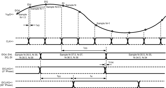 Figure 1. Clocking in 1:4 Demux DES Mode
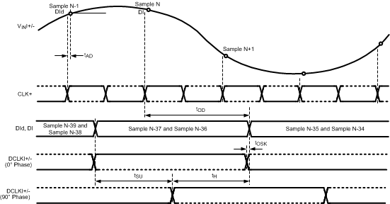 Figure 2. Clocking in 1:2 Demux Non-DES Mode*
* The timing here is shown for the I channel only. However, the Q channel functions precisely the same as the I channel, with VinQ+, VinQ–, DCLKQ+, DCLKQ–, DQd and DQ instead of VinI+, VinI–, DCLKI+, DCLKI–, DId and DI. Both the I channel and the Q channel use the same CLK+, CLK–.
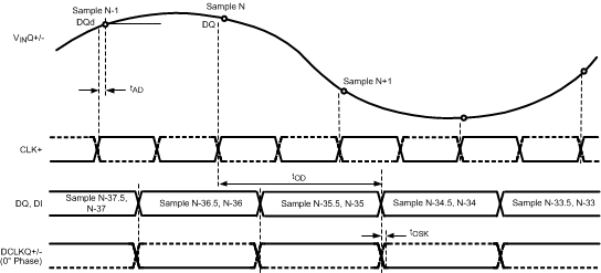 Figure 3. Clocking in Non-Demux Mode Non-DES Mode**
** The timing here is shown for the Q channel only. However, for the non-demux non-DES node, either the I channel and the Q channel may be used as input. For this case, the I-channel functions precisely the same as those of the Q channel, with VinI+, VinI–, DCLKI+, DCLKI–, and DI instead of VinQ+, VinQ–, DCLKQ+, DCLKQ–, and DQ. Both the I channel and Q channel use the same CLK+, CLK–.
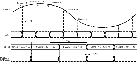 Figure 4. Clocking in Non-Demux Mode DES Mode
 Figure 5. Data Clock Reset Timing
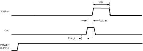 Figure 6. On-Command Calibration Timing
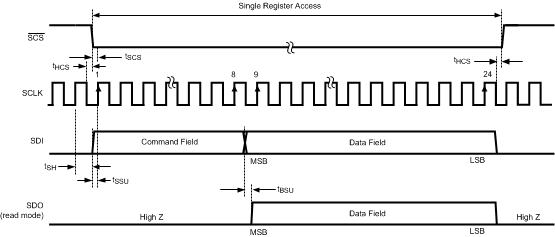 Figure 7. Serial Interface Timing
6.18 Typical Characteristics
VA = VDR = VTC = VE = 1.9 V, fCLK = 1000 MHz, fIN = 498 MHz, TA= 25°C, I channel and Q channel, unused channel terminated to AC ground and 1:2 demux non-DES mode (1:1 demux mode has similar performance), unless otherwise stated. NPR plots Notch fC = 325 MHz and Notch width = 25 MHz.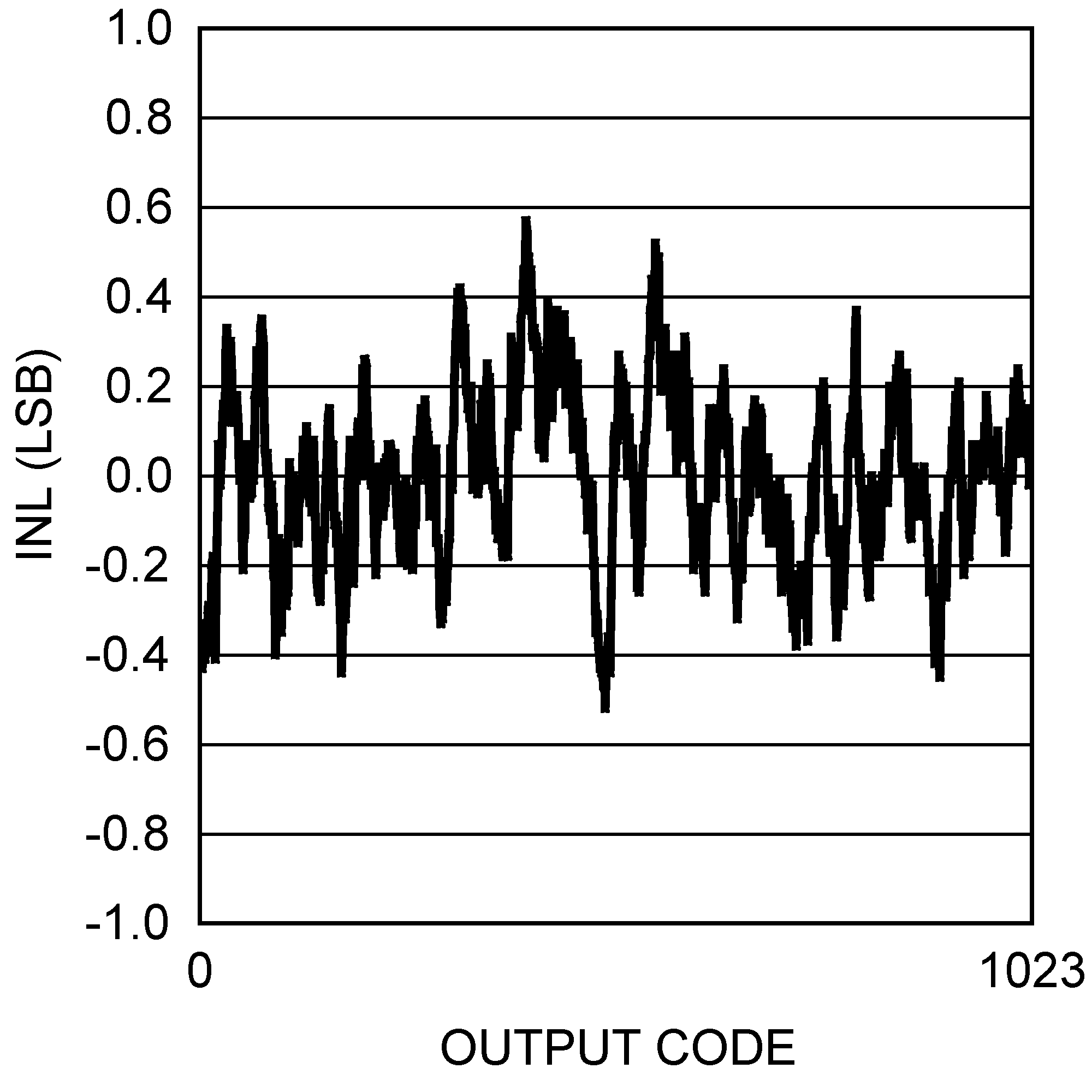 Figure 8. INL vs Code
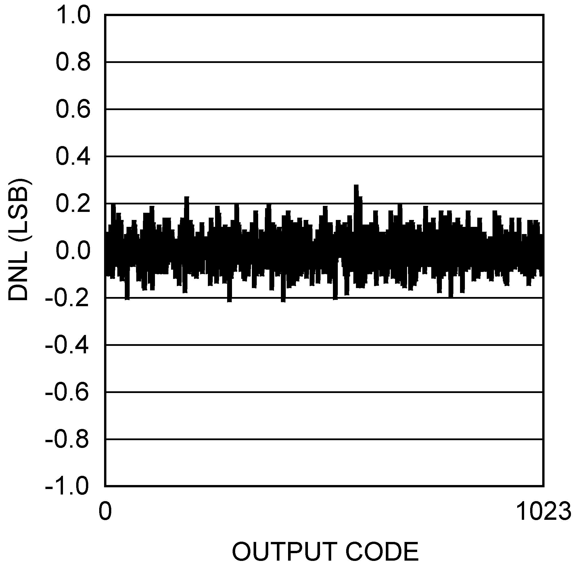 Figure 10. DNL vs Code
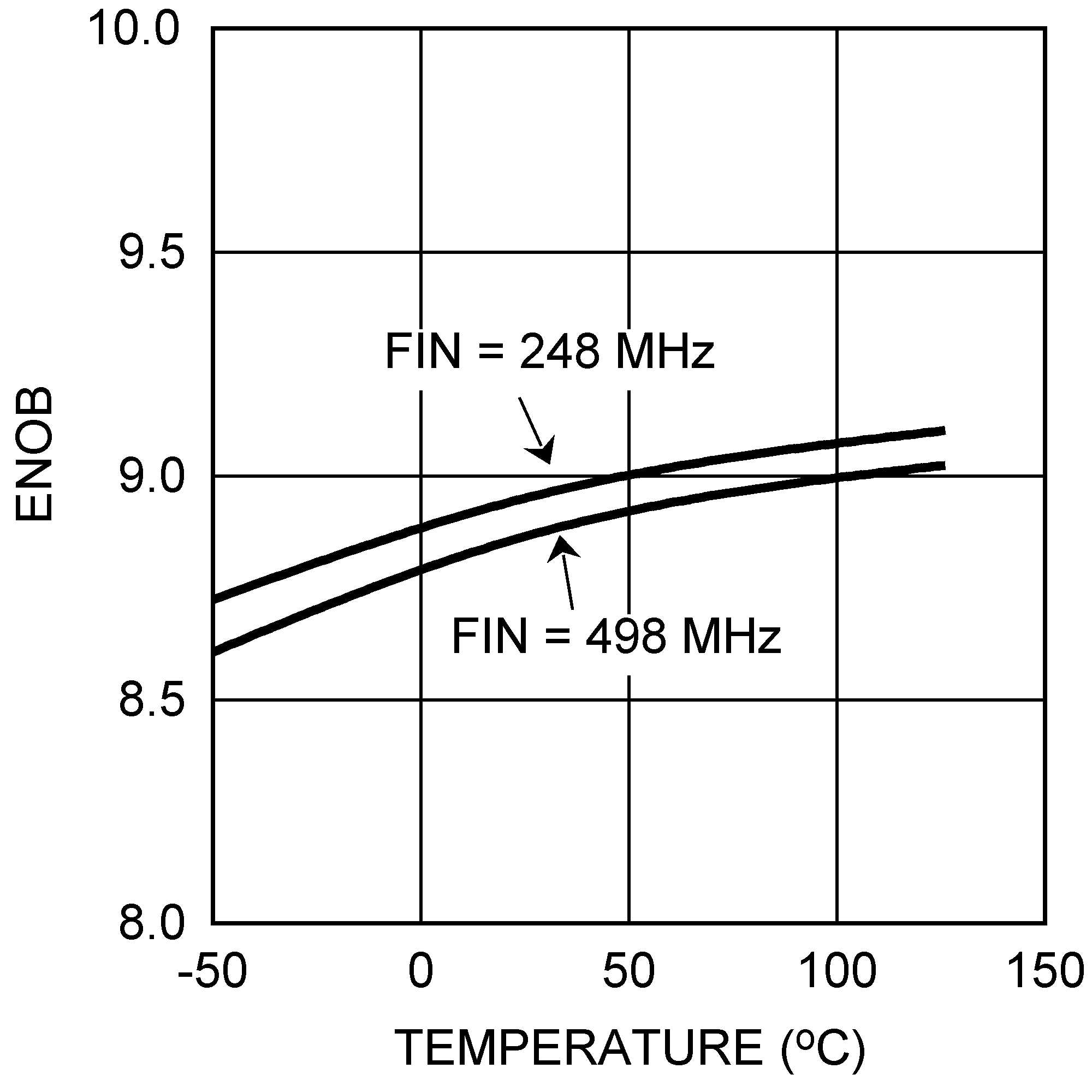 Figure 12. ENOB vs Temperature
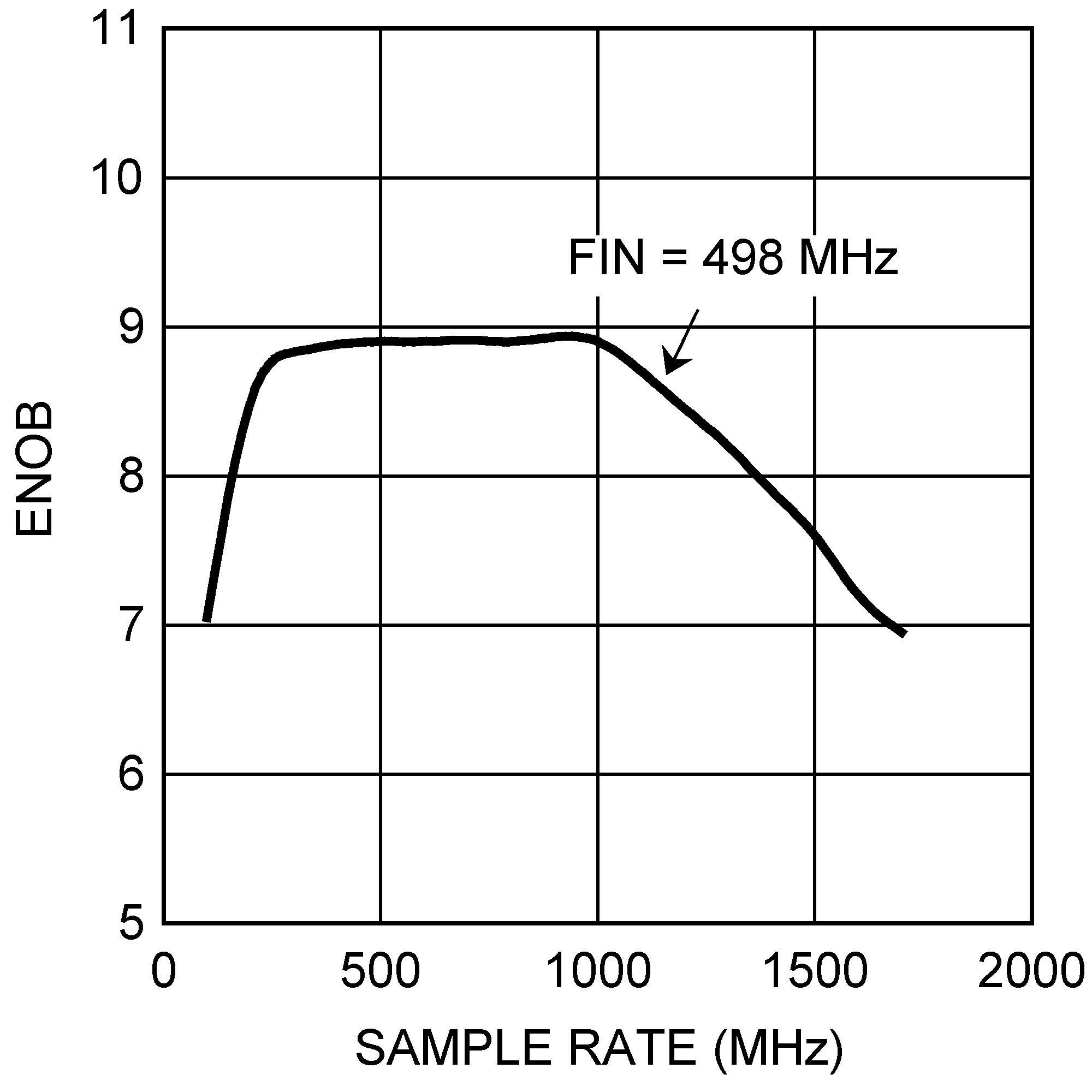 Figure 14. ENOB vs Clock Frequency
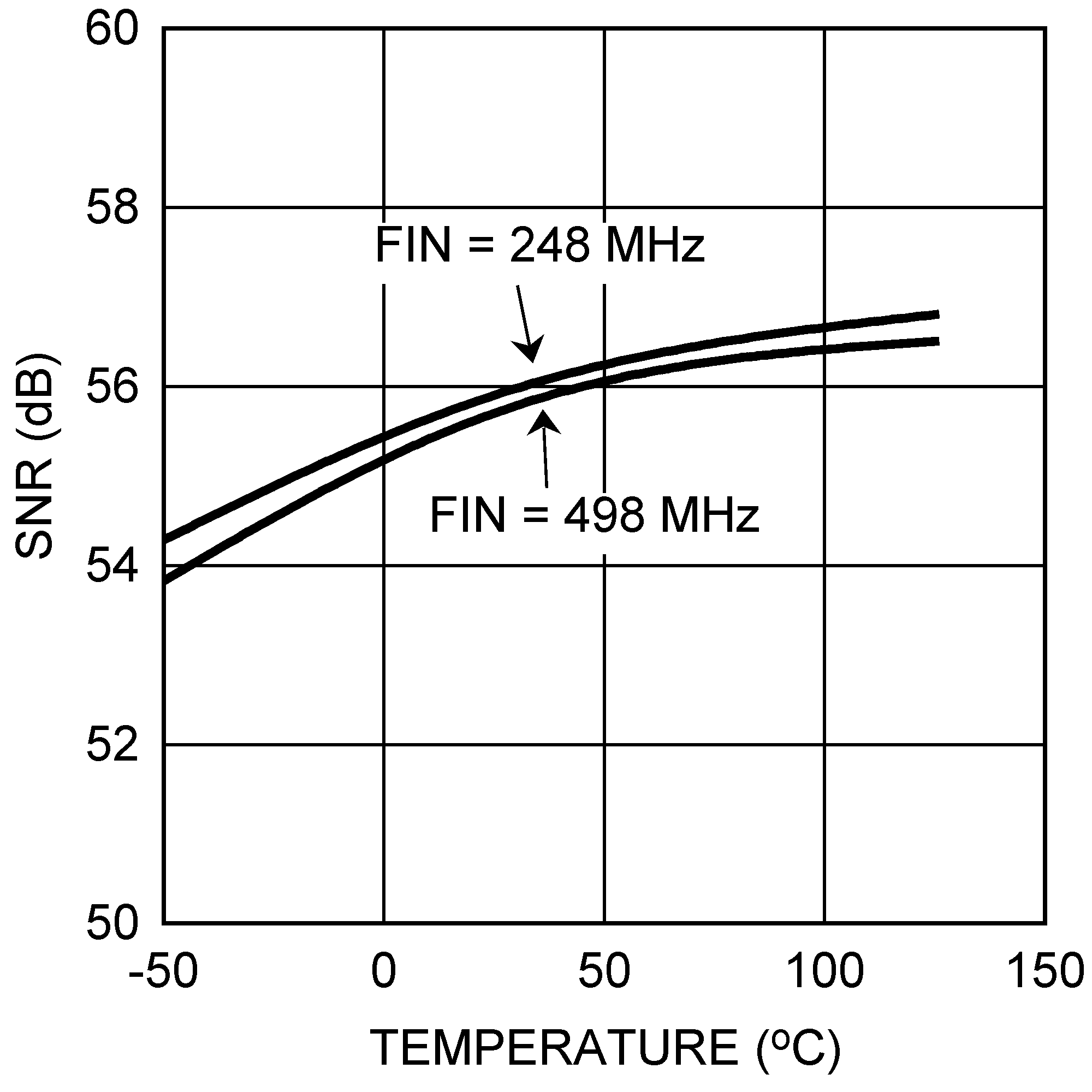 Figure 16. SNR vs Temperature
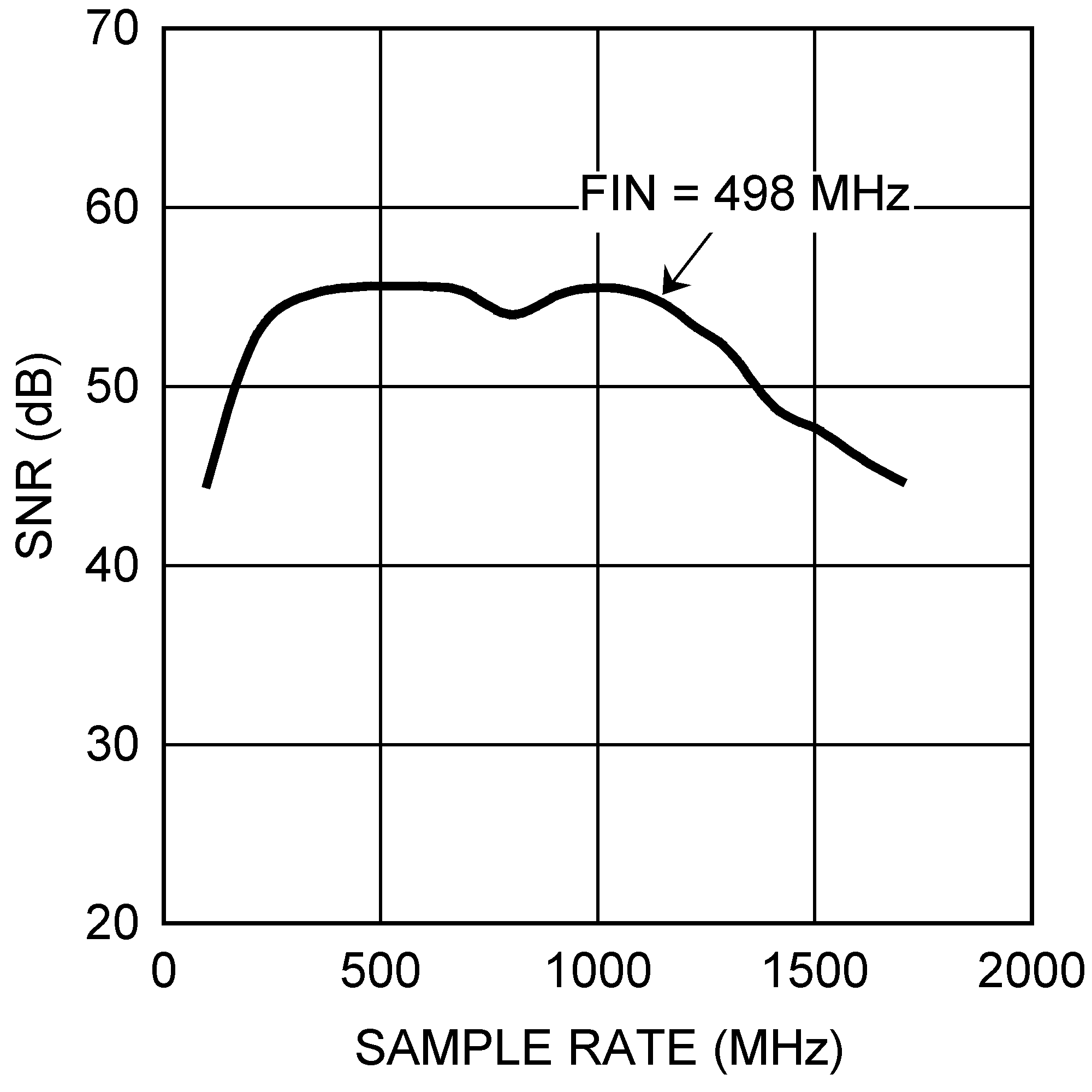 Figure 18. SNR vs Clock Frequency
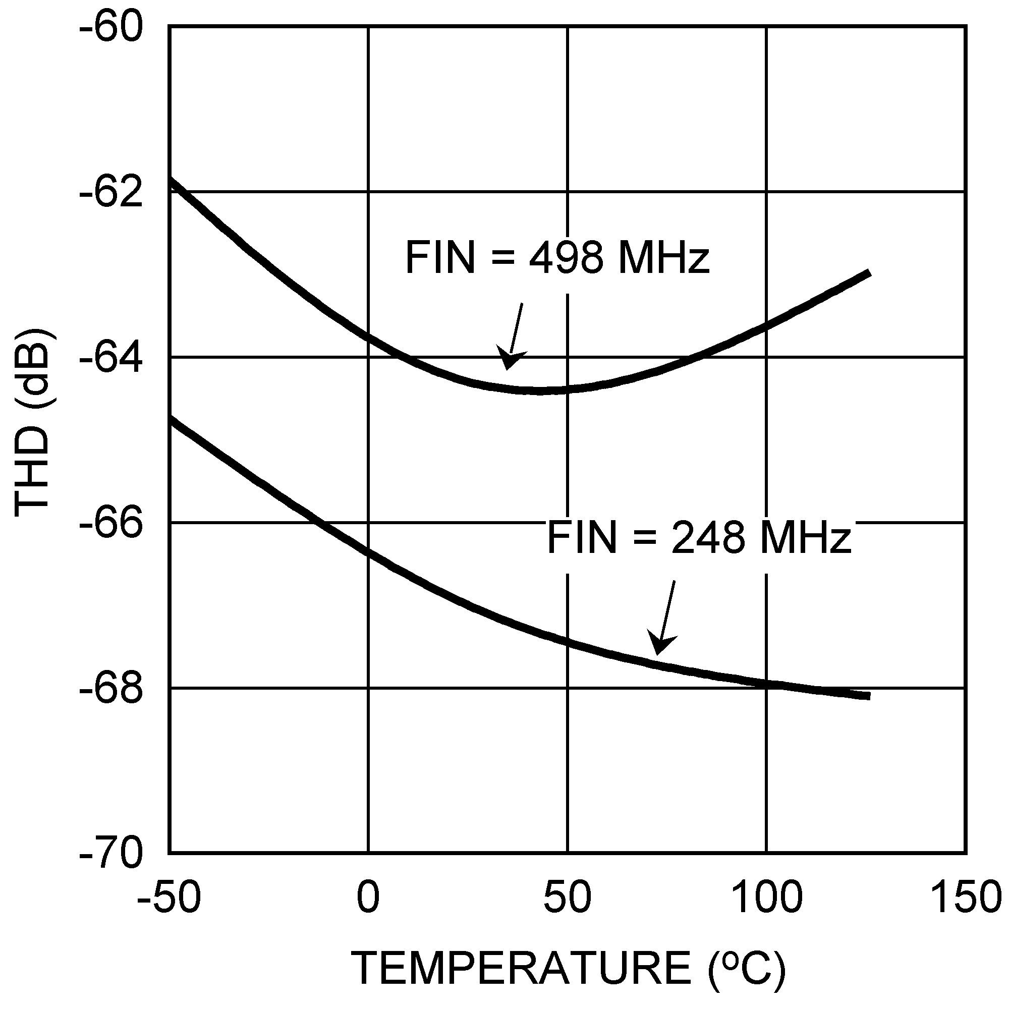 Figure 20. THD vs Temperature
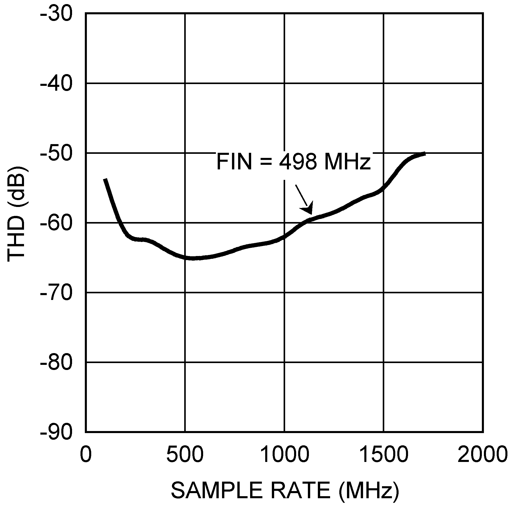 Figure 22. THD vs Clock Frequency
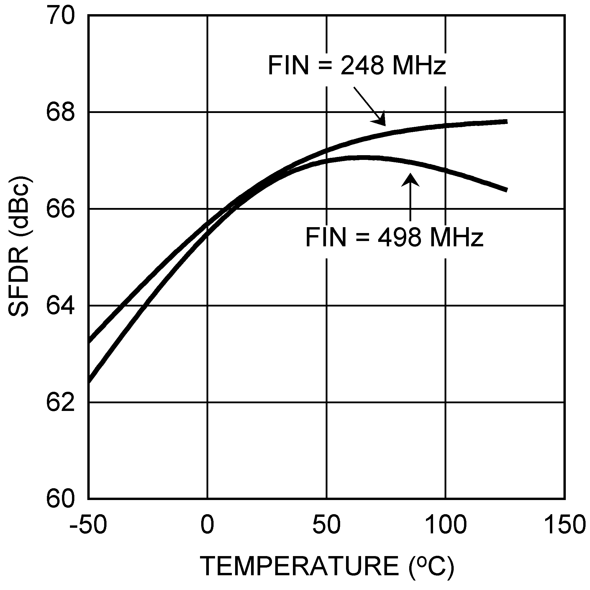 Figure 24. SFDR vs Temperature
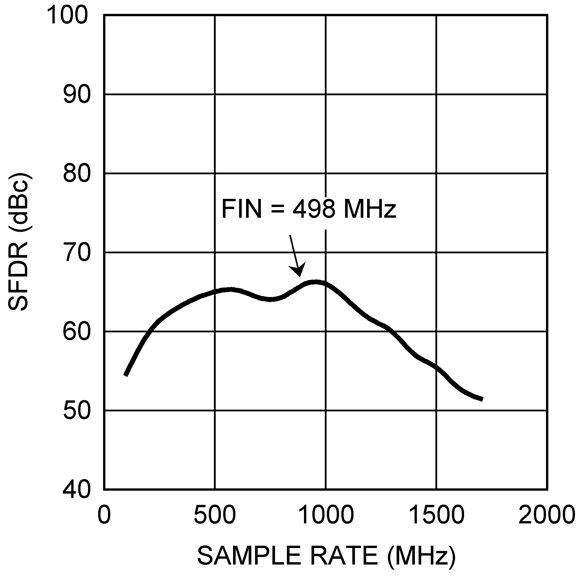 Figure 26. SFDR vs Clock Frequency
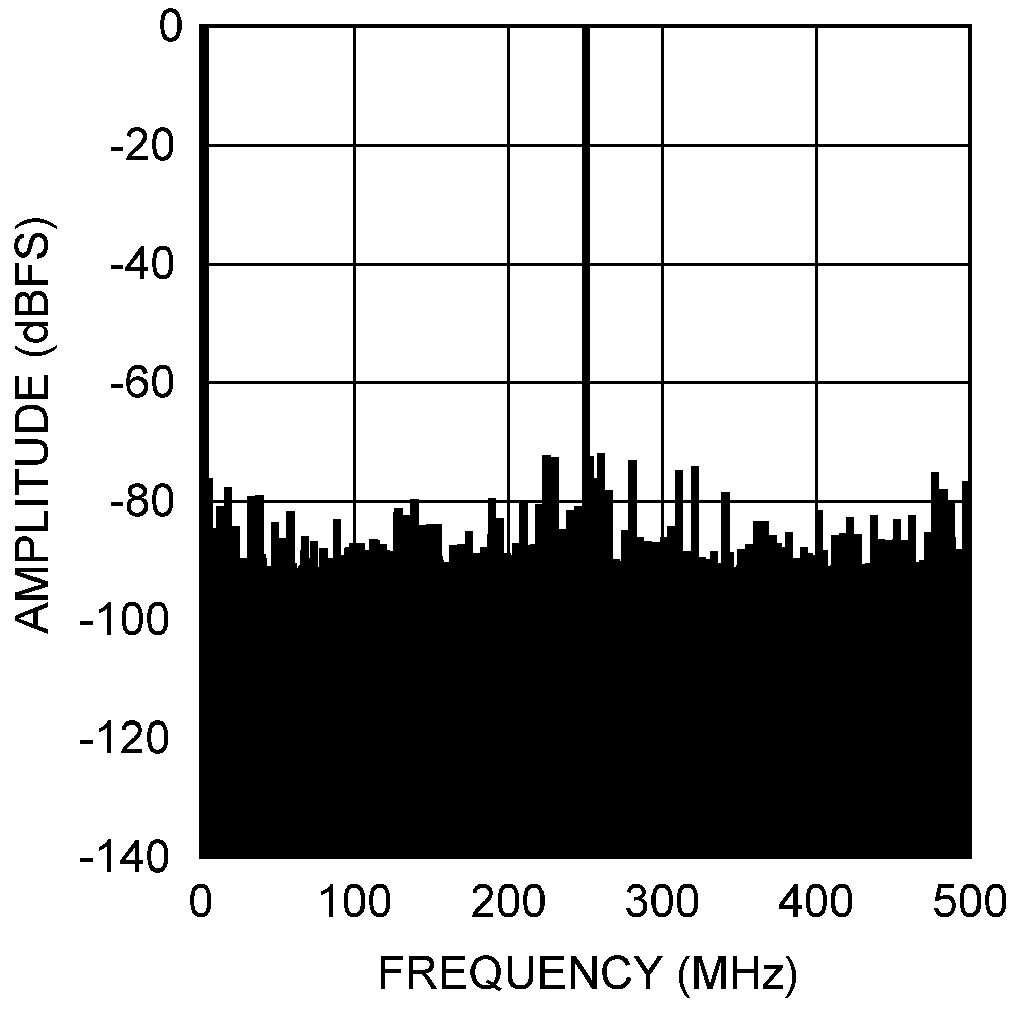 Figure 28. Spectral Response at FIN = 248 MHz
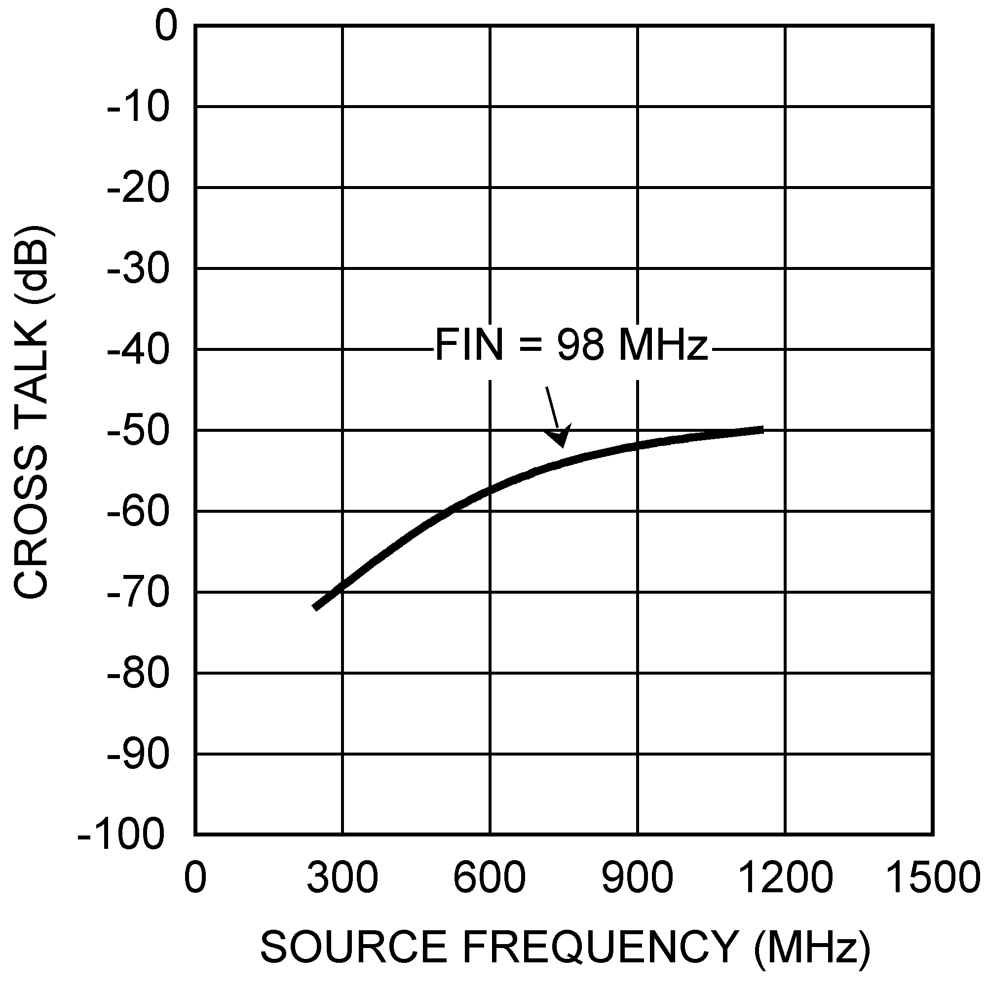 Figure 30. Crosstalk vs Source Frequency
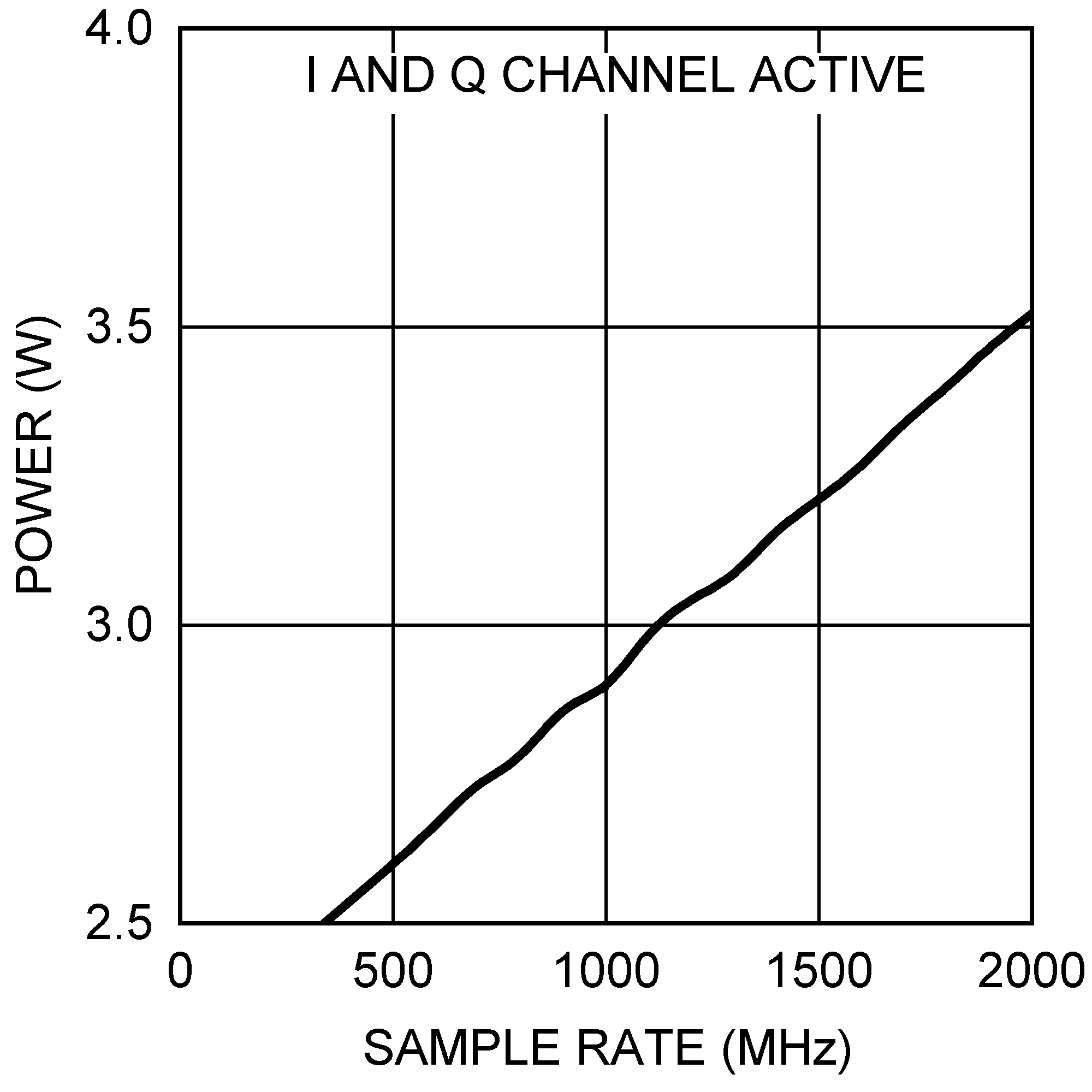 Figure 32. Power Consumption vs Clock Frequency
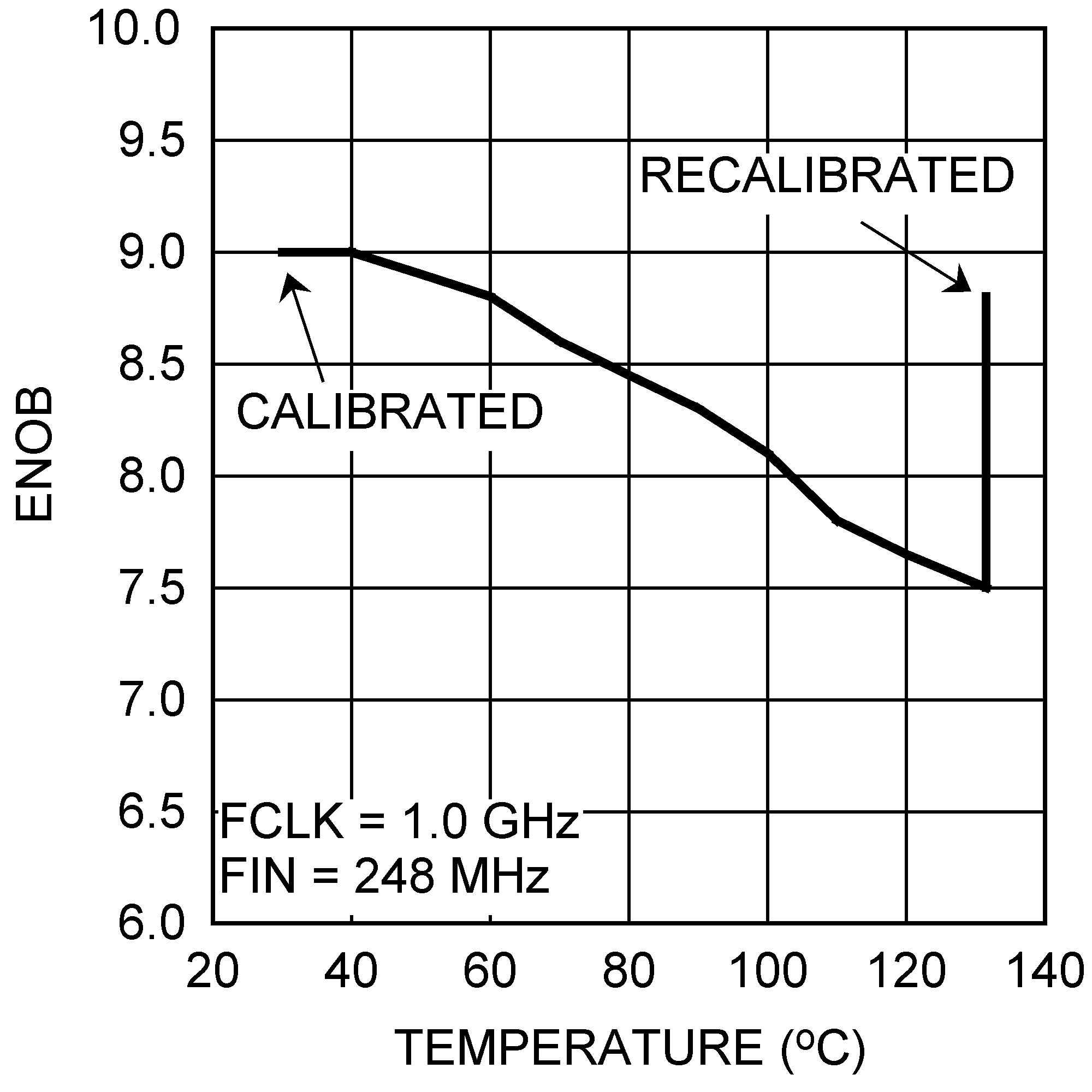 Figure 34. Gain vs Temperature ENOB
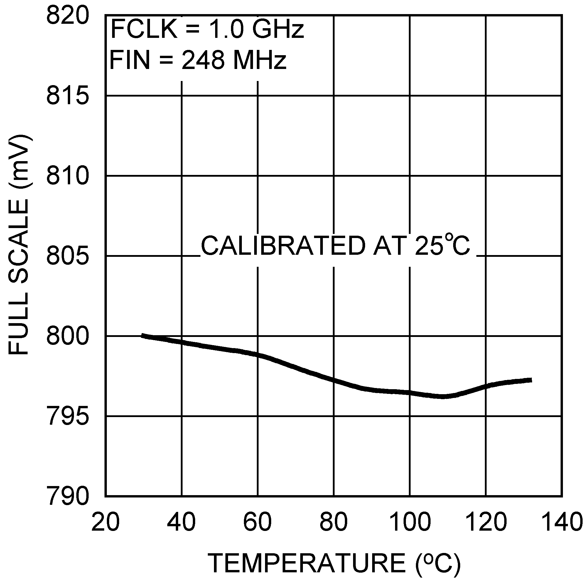 Figure 36. NPR vs fC Notch
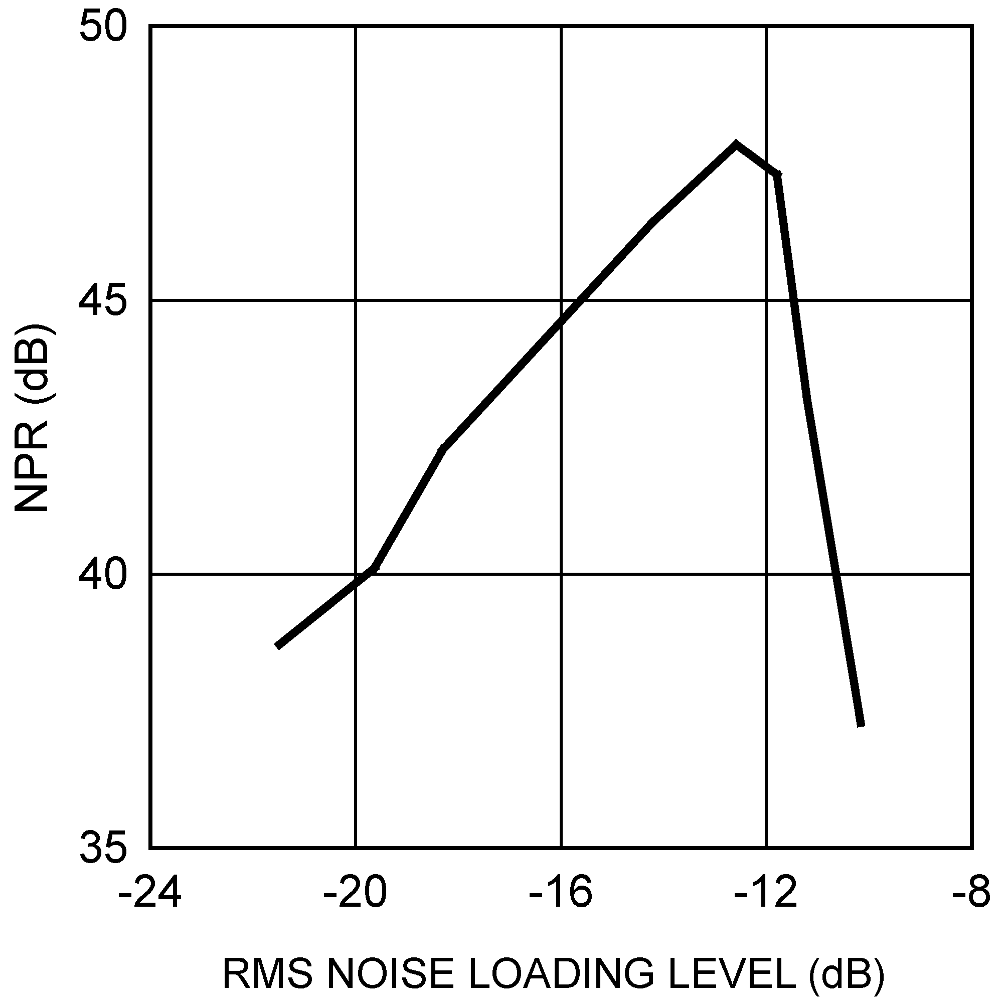 Figure 38. NPR vs RMS Noise Loading Level
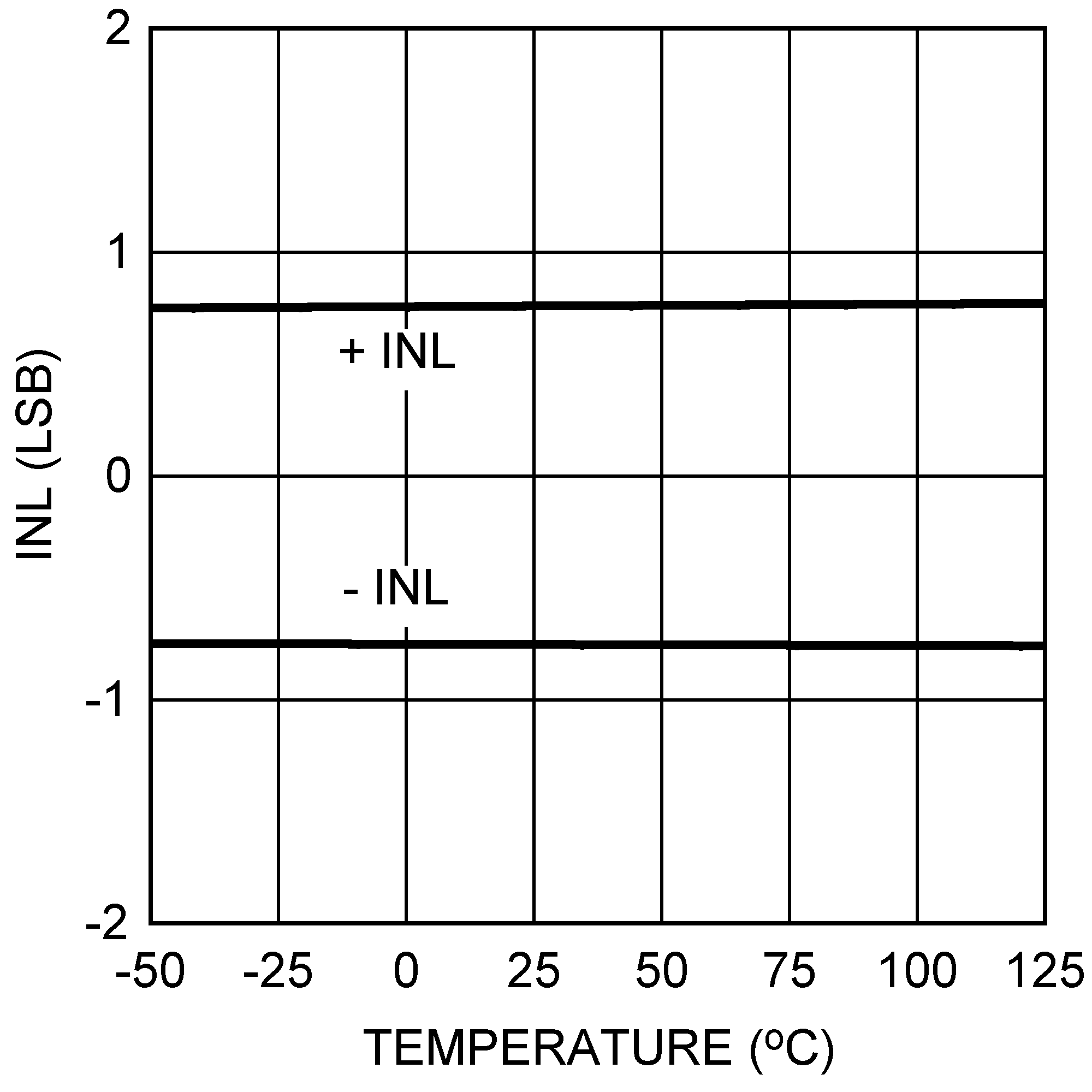 Figure 9. INL vs Temperature
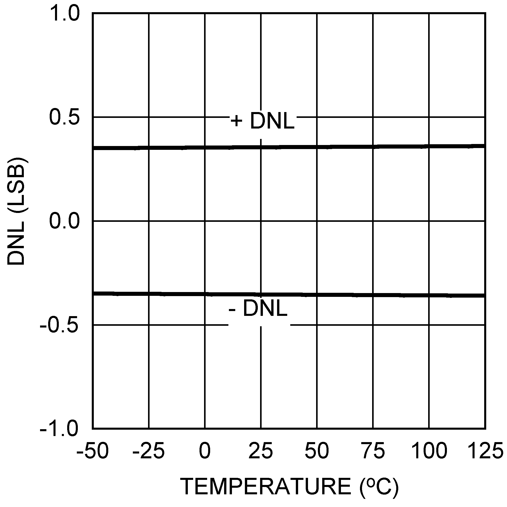 Figure 11. DNL vs Temperature
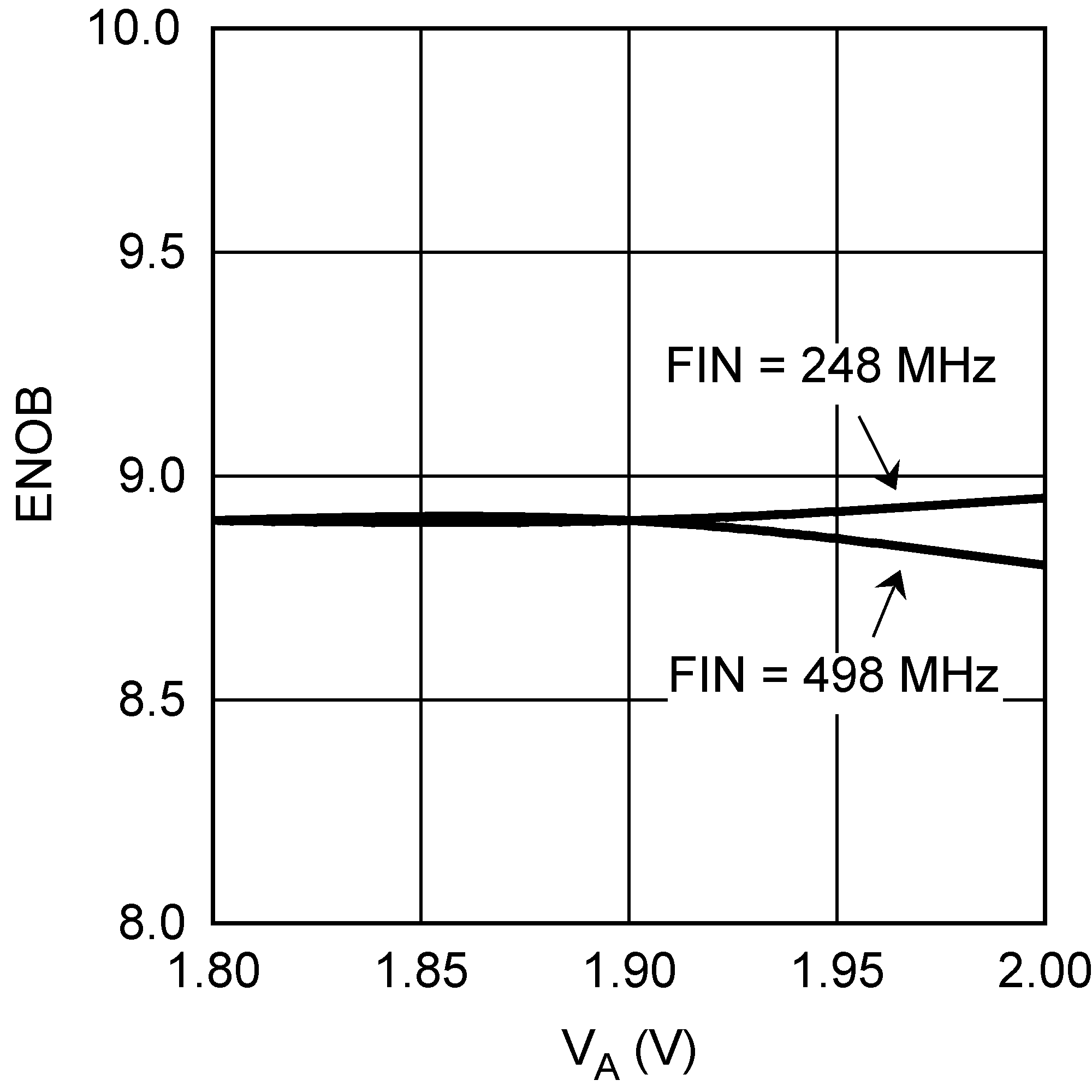 Figure 13. ENOB vs Supply Voltage
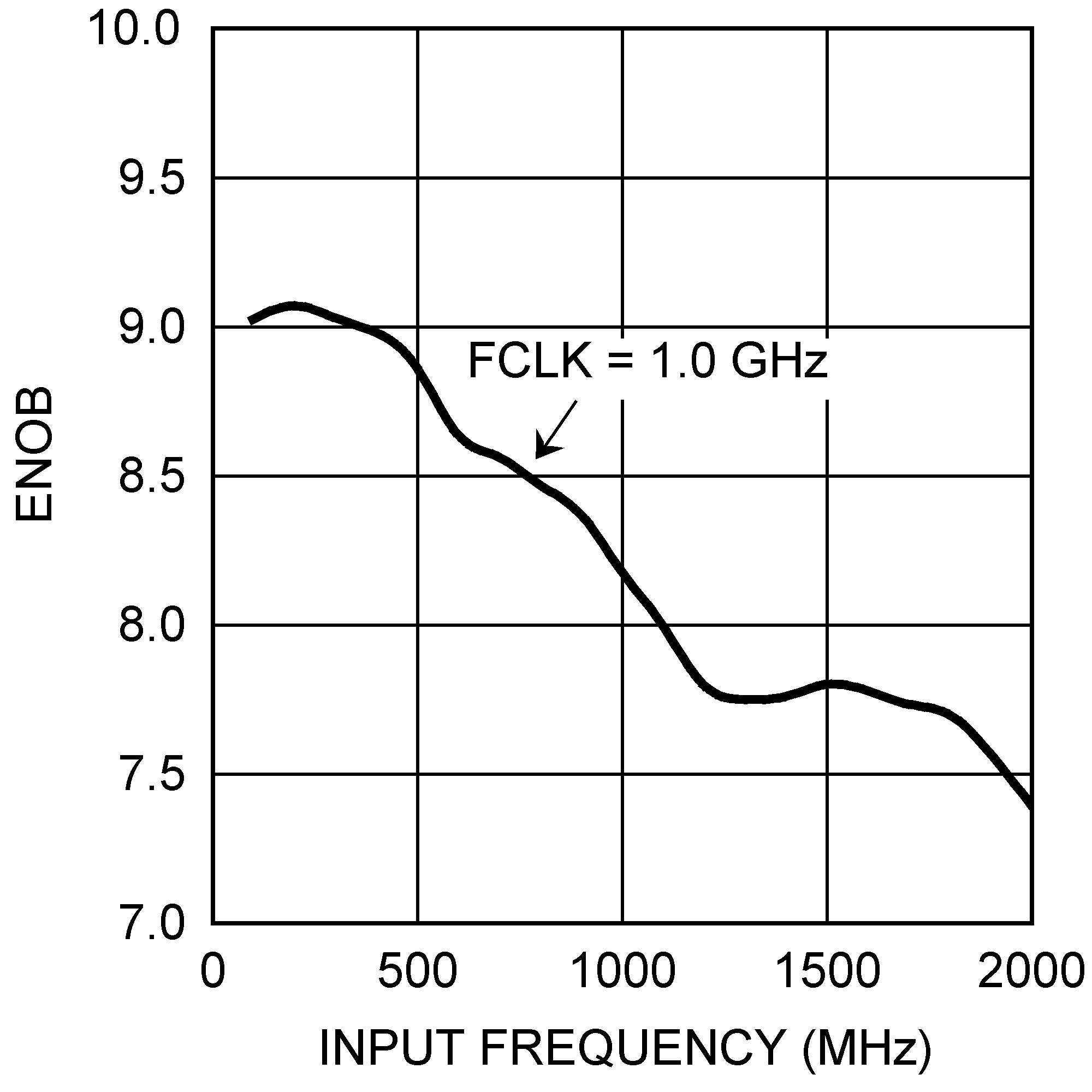 Figure 15. ENOB vs Input Frequency
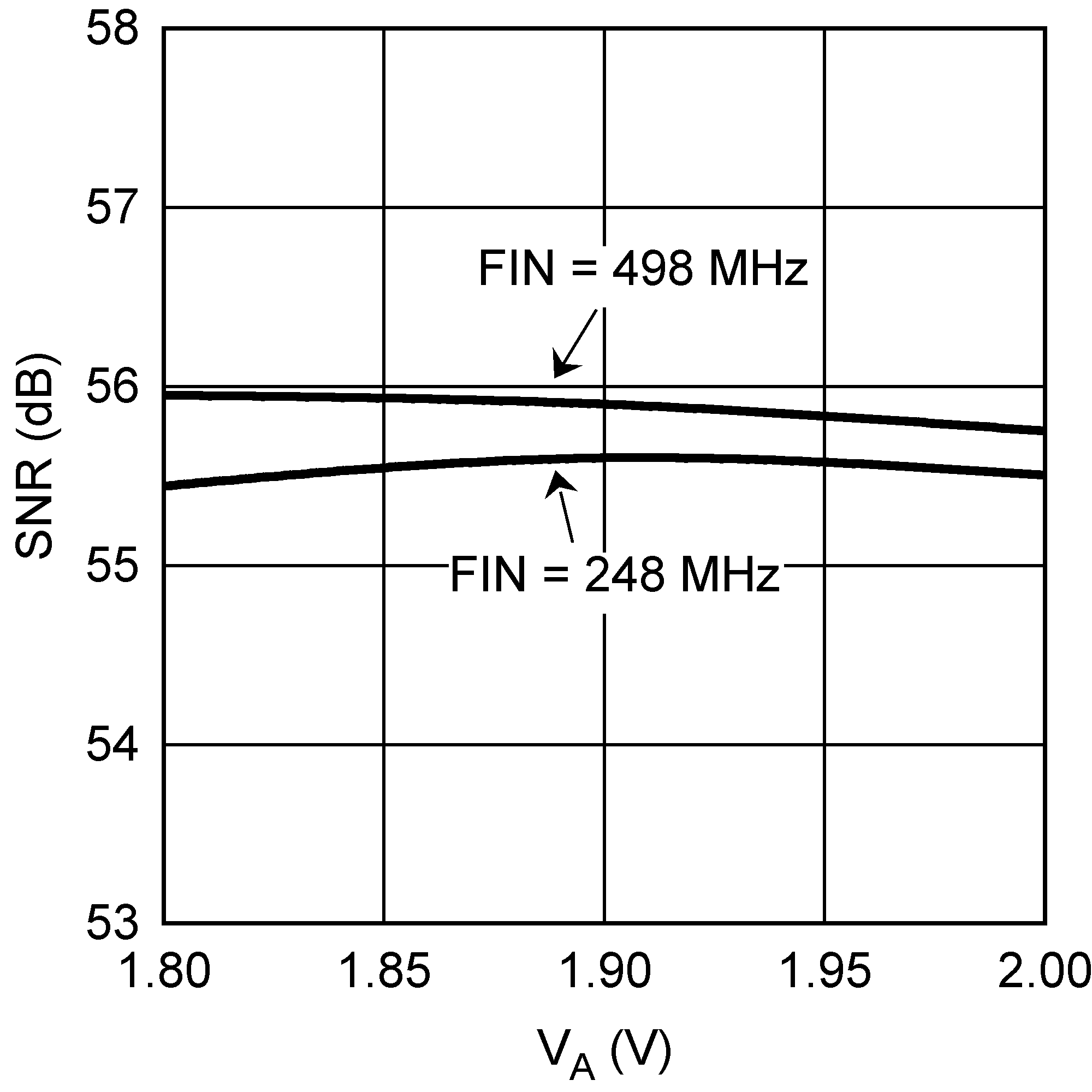 Figure 17. SNR vs Supply Voltage
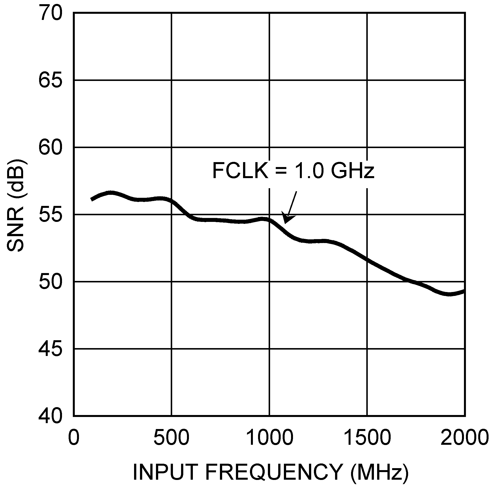 Figure 19. SNR vs Input Frequency
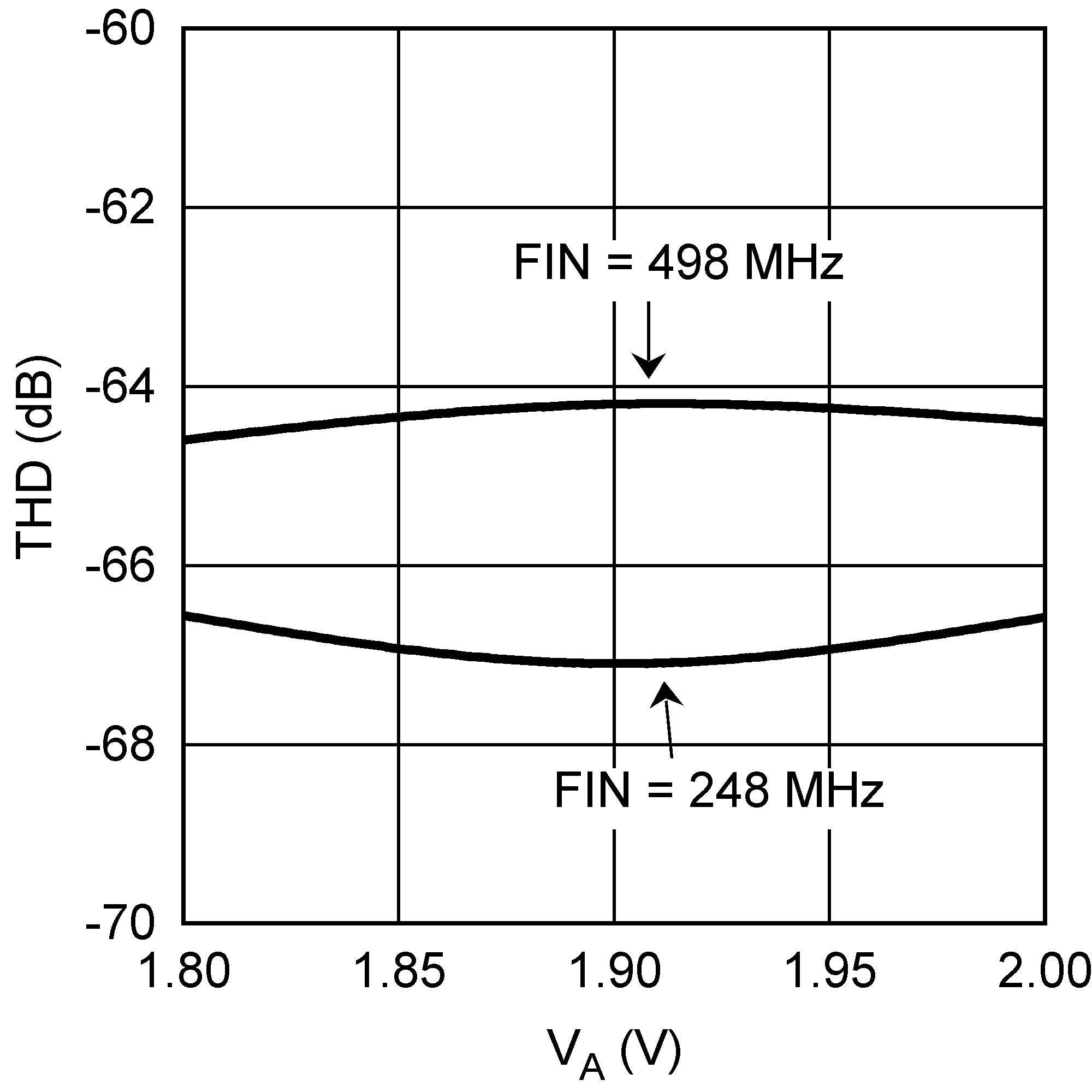 Figure 21. THD vs Supply Voltage
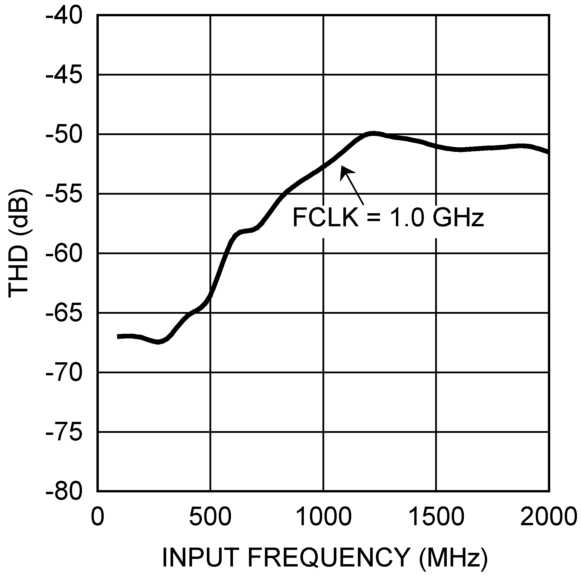 Figure 23. THD vs Input Frequency
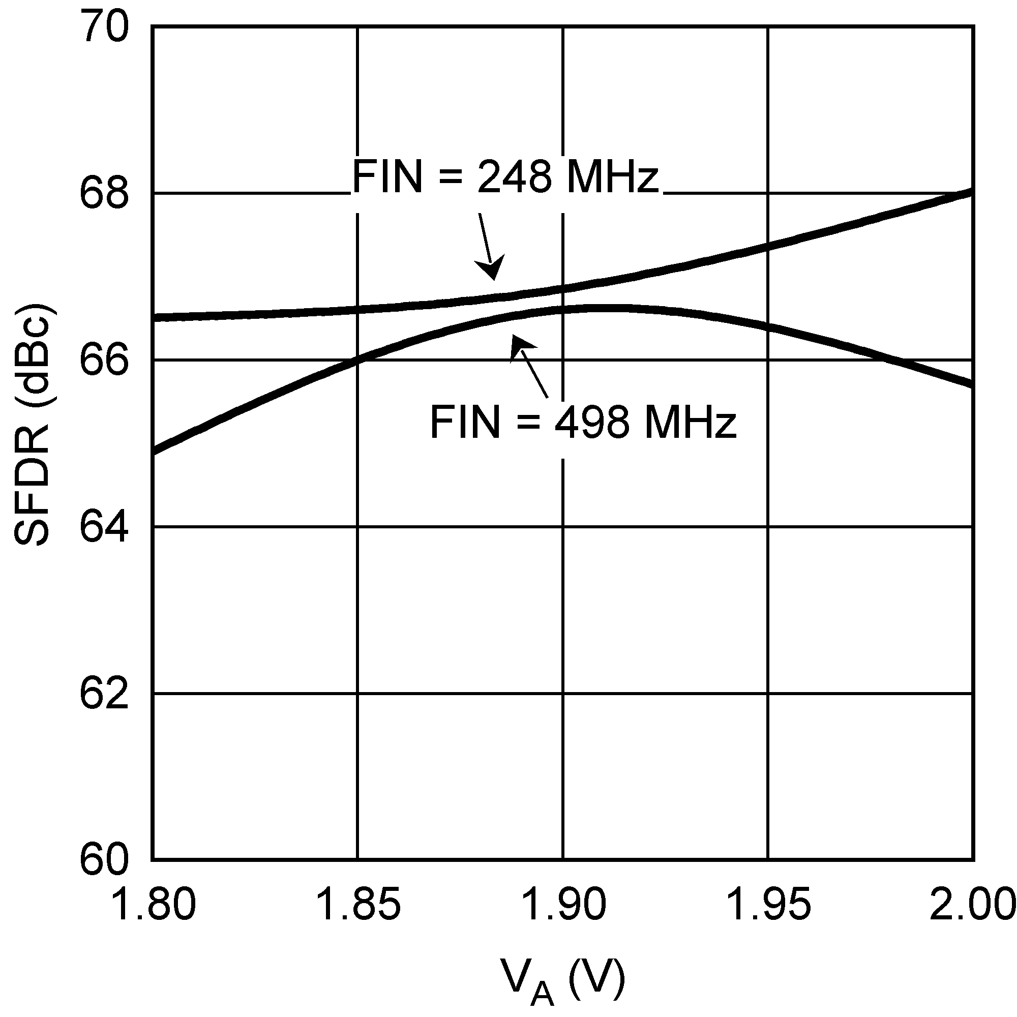 Figure 25. SFDR vs Supply Voltage
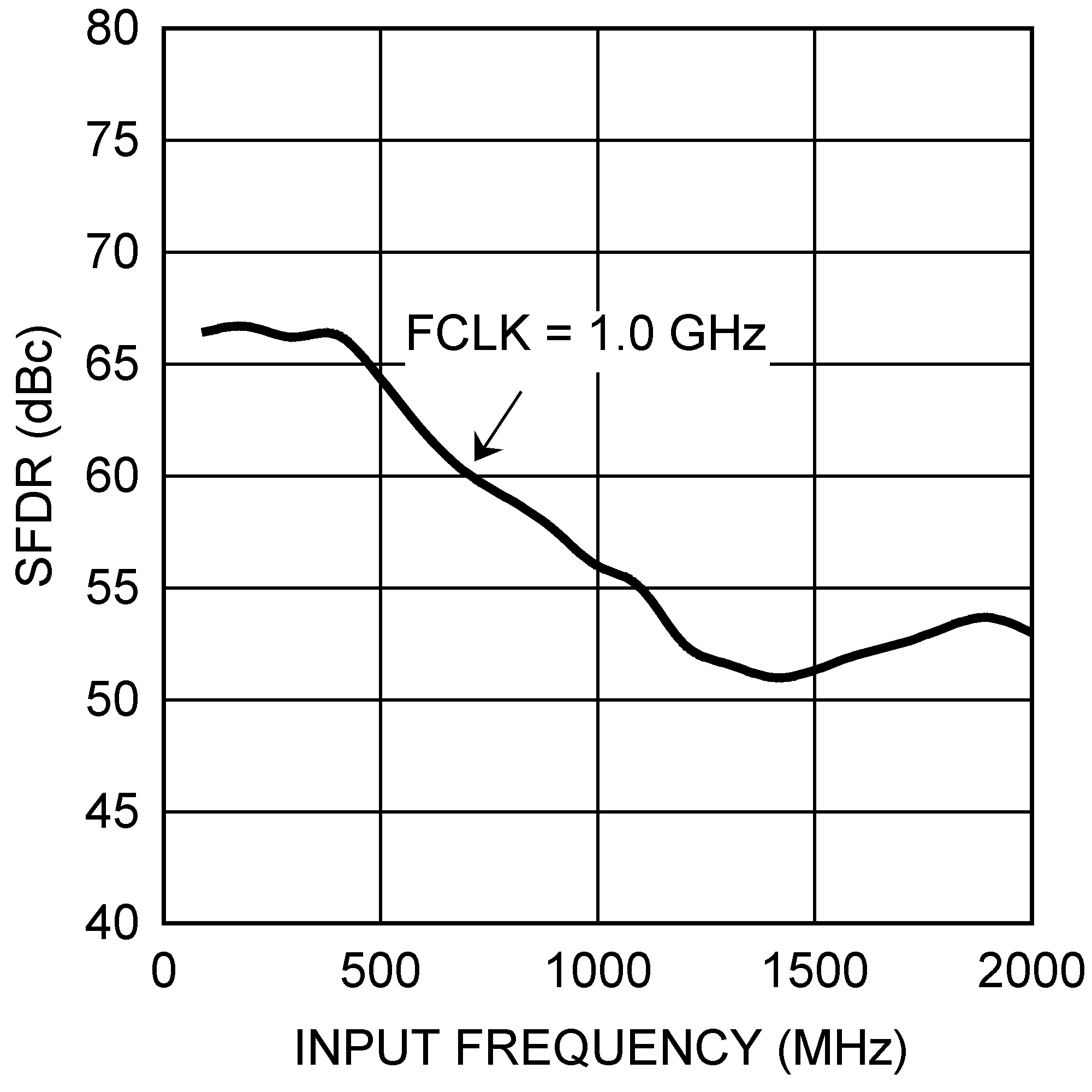 Figure 27. SFDR vs Input Frequency
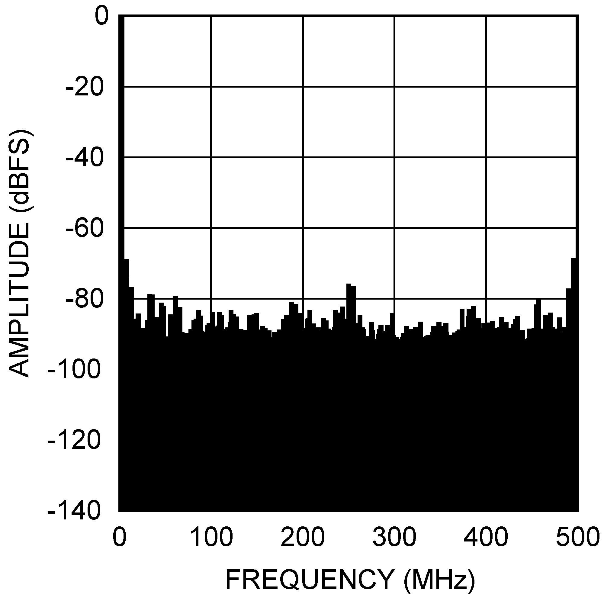 Figure 29. Spectral Response at FIN = 498 MHz
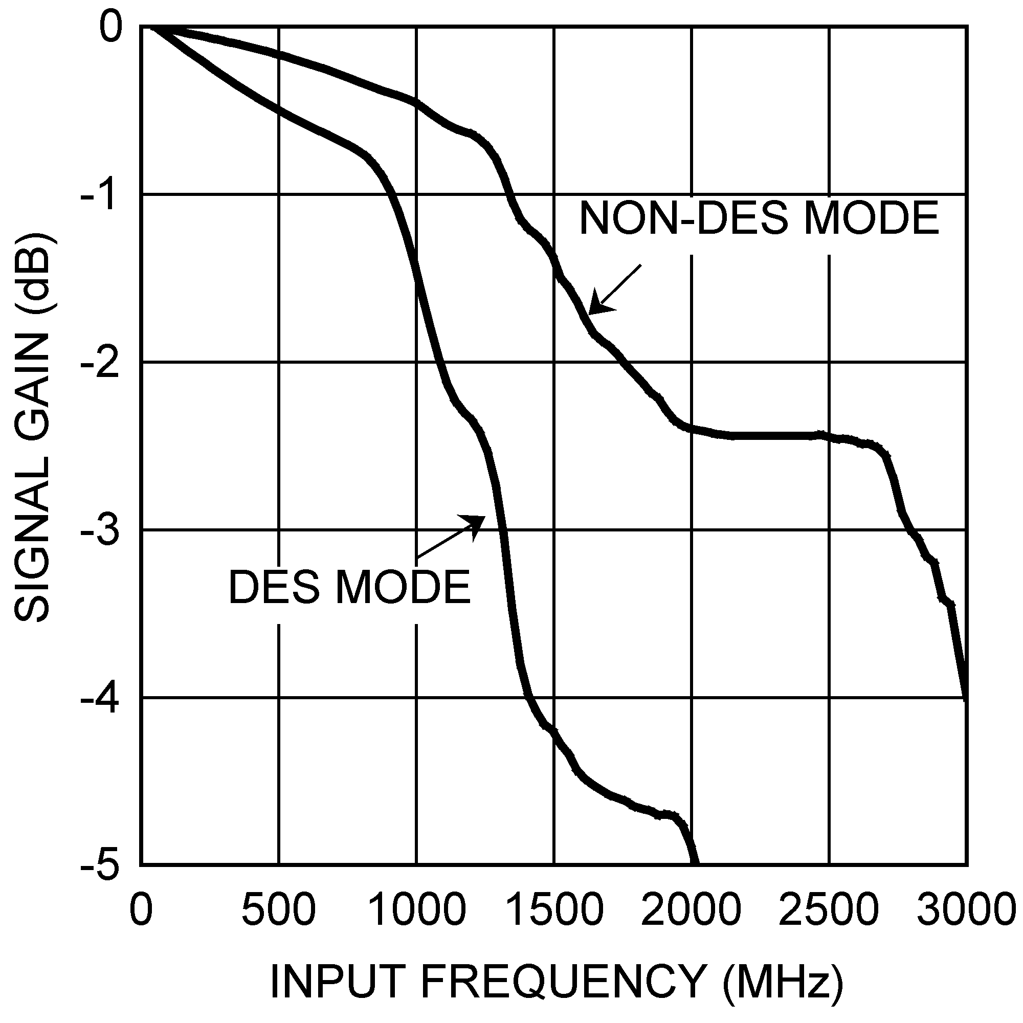 Figure 31. Full Power Bandwidth
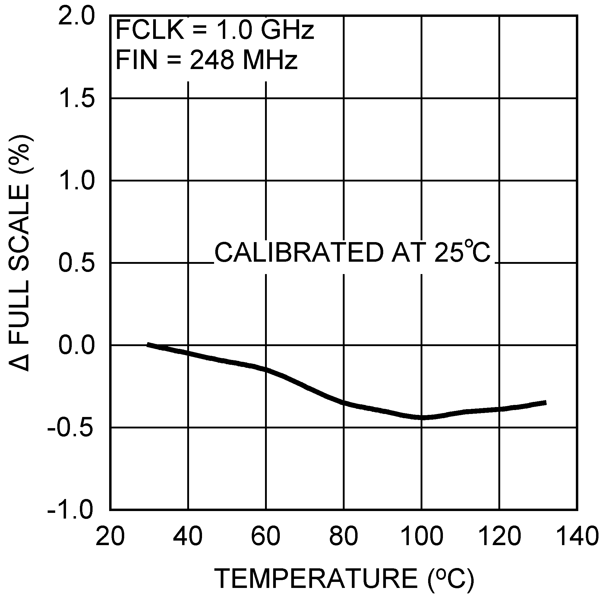 Figure 33. Gain vs Temperature FS Percent Change
 Figure 35. Gain vs Temperature FS
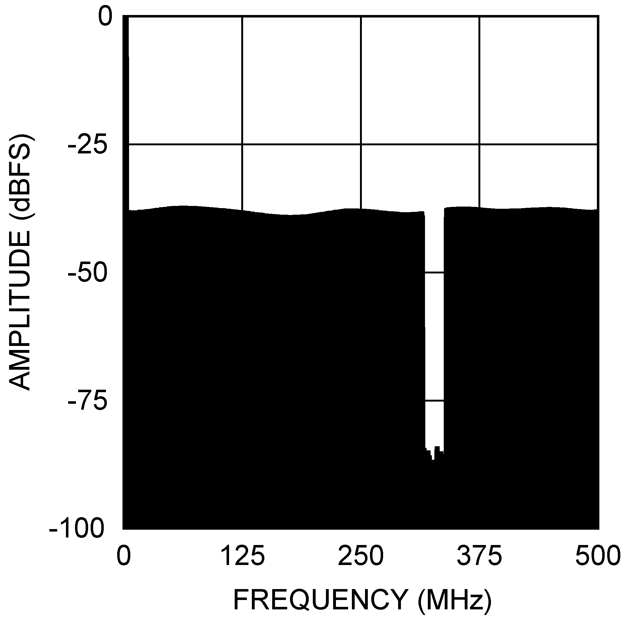 Figure 37. Amplitude vs Frequency