SBVS191B April 2012 – August 2014
PRODUCTION DATA.
1 Features
- 200-mA Low-Dropout Regulator with EN
- Multiple Output Voltage Versions Available:
- TPS799L: Fixed Outputs of 5.2 V to 6.2 V Using Innovative Factory EEPROM Programming
- TPS799L57: 5.7-V Output
- TPS799L54: 5.4-V Output
- TPS799: Output Options Less Than 5.2 V
- Inrush current Protection with EN Toggle
- Low IQ: 40 μA
- High PSRR: 66 dB at 1 kHz
- Stable with a Low-ESR, 2.0-μF Typical Output Capacitance
- Excellent Load and Line Transient Response
- 2% Overall Accuracy (Load, Line, and Temperature)
- Very Low Dropout: 100 mV
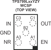
- Package: 5-Bump, Thin, 1-mm × 1.37-mm DSBGA
2 Applications
- Cellular Phones
- Wireless LAN, Bluetooth®
- VCOs, RF
- Handheld Organizers, PDAs
3 Description
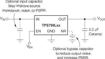
The TPS799L family of low-dropout (LDO), low-power linear regulators offers excellent ac performance with very low ground current. High power-supply rejection ratio (PSRR), low noise, fast start-up, and excellent line and load transient response are provided while consuming a very low 40-μA (typical) ground current.
The TPS799Lxx is stable with ceramic capacitors and uses an advanced BiCMOS fabrication process to yield a dropout voltage of typically 100 mV at a
200-mA output. The TPS799L uses a precision voltage reference and feedback loop to achieve an overall accuracy of 2% over all load, line, process, and temperature variations. The TPS799L features inrush current protection when the EN toggle is used to start the device, immediately clamping the current.
All devices are fully specified over the temperature range of TJ = –40°C to 125°C, and offered in a low-profile, die-sized ball grid array (DSBGA) package, ideal for wireless handsets and WLAN cards.
Device Information(1)
| PART NUMBER | PACKAGE | BODY SIZE (NOM) |
|---|---|---|
| TPS799Lxx | DSBGA (5) | 1.57 mm × 1.20 mm |
- For all available packages, see the package option addendum at the end of the datasheet.
Typical Application Circuit
4 Revision History
Changes from A Revision (July 2012) to B Revision
- Changed document format; added new sections and moved existing sectionsGo
- Added TPS799L54 device to data sheetGo
- Changed WCSP package name to DSBGA throughout data sheetGo
- Changed free-air to junction in Absolute Maximum Ratings table conditionsGo
- Changed free-air to junction in Recommended Operating Conditions table conditionsGo
- Deleted Start-up time symbolGo
Changes from * Revision (April 2012) to A Revision
- Deleted Figure 19Go