SBVS191B April 2012 – August 2014
PRODUCTION DATA.
7 Detailed Description
7.1 Overview
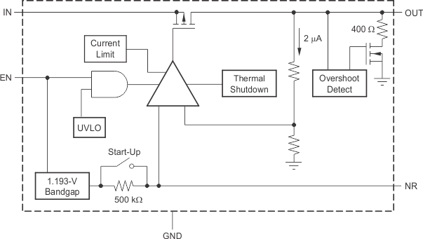
The TPS799Lxx family of low-dropout (LDO) regulators combines the high performance required of many RF and precision analog applications with ultralow current consumption. High PSRR is provided by a high-gain, high-bandwidth error loop with good supply rejection at very low headroom (VIN – VOUT). A noise-reduction pin is provided to bypass noise generated by the band-gap reference and to improve PSRR, while a quick-start circuit quickly charges this capacitor at start-up. The combination of high performance and low ground current also make these devices an excellent choice for portable applications. All versions have thermal and overcurrent protection, and are fully specified from –40°C to 125°C.
The TPS799Lxx family also features inrush current protection with an EN toggle start-up, and overshoot detection at the output. When the EN toggle is used to start the device, current limit protection is immediately activated, restricting the inrush current to the device (see Figure 16). If voltage at the output overshoots 5% from the nominal value, a pull-down resistor reduces the voltage to normal operating conditions, as shown in the Functional Block Diagram.
7.2 Functional Block Diagram
7.3 Feature Description
7.3.1 Internal Current Limit
The TPS799Lxx internal current limit helps protect the regulator during fault conditions. In current limit mode, the output sources a fixed amount of current that is largely independent of the output voltage. For reliable operation, do not operate the device in a current-limit state for extended periods of time.
The PMOS pass element in the TPS799Lxx has a built-in body diode that conducts current when the voltage at OUT exceeds the voltage at IN. This current is not limited; therefore, if extended reverse voltage operation is anticipated, external limiting may be required.
7.3.2 Shutdown
The enable pin (EN) is active high and is compatible with standard and low-voltage TTL-CMOS levels. When shutdown capability is not required, EN can be connected to IN.
7.3.3 Start Up
The TPS799Lxx uses a start-up circuit to quickly charge the noise reduction capacitor, CNR, if present (see the Functional Block Diagram). This circuit allows for the combination of very low output noise and fast start-up times. The NR pin is high impedance so a low leakage CNR capacitor must be used; most ceramic capacitors are appropriate for this configuration.
Note that for fastest start-up, apply VIN first, and then drive the enable pin (EN) high. If EN is tied to IN, start-up is somewhat slower. The start-up switch is closed for approximately 135 μs. To ensure that CNR is fully charged during start-up, use a 0.01-μF or smaller capacitor.
7.3.4 Undervoltage Lockout (UVLO)
The TPS799Lxx uses an undervoltage lockout circuit to keep the output shut off until internal circuitry is operating properly. The UVLO circuit has a deglitch feature so that undershoot transients are typically ignored on the input if these transients are less than 50 μs in duration.
7.4 Device Functional Modes
Driving EN over 1.2 V turns on the regulator. Driving EN below 0.4 V puts the regulator into shutdown mode, thus reducing the operating current to 150 nA, nominal.