SBVS191B April 2012 – August 2014
PRODUCTION DATA.
8 Application and Implementation
8.1 Application Information
The TPS799Lxx family of LDO regulators provides high PSRR while maintaining ultralow current consumption. The family also features inrush current protection and overshoot detection at the output.
8.2 Typical Application
Figure 17 shows the basic circuit connections.
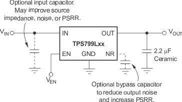 Figure 17. Typical Application Circuit
8.2.1 Design Requirements
8.2.1.1 Input and Output Capacitor Requirements
Although an input capacitor is not required for stability, good analog design practice is to connect a 0.1-μF to
1-μF low ESR capacitor across the input supply near the regulator. This capacitor counteracts reactive input sources and improves transient response, noise rejection, and ripple rejection. A higher-value capacitor may be necessary if large, fast rise-time load transients are anticipated, or if the device is located several inches from the power source. If source impedance is not sufficiently low, a 0.1-μF input capacitor may be necessary to ensure stability.
The TPS799Lxx is designed to be stable with standard ceramic capacitors with values of 2.2 μF or greater. X5R- and X7R-type capacitors are best because they have minimal variation in value and ESR over temperature. Maximum ESR must be less than 1.0 Ω.
8.2.1.2 Output Noise
In most LDOs, the band gap is the dominant noise source. If a noise-reduction capacitor (CNR) is used with the TPS799Lxx, the band gap does not contribute significantly to noise. Instead, noise is dominated by the output resistor divider and the error amplifier input. To minimize noise in a given application, use a 0.01-μF noise reduction capacitor. To further optimize noise, equivalent series resistance of the output capacitor can be set to approximately 0.2 Ω. This configuration maximizes phase margin in the control loop, reducing total output noise by up to 10%.
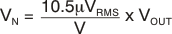
Noise can be referred to the feedback point; with CNR = 0.01 μF total noise is approximately given by Equation 1:
8.2.1.3 Dropout Voltage
The TPS799Lxx uses a PMOS pass transistor to achieve a low dropout voltage. When (VIN – VOUT) is less than the dropout voltage (VDO), the PMOS pass device is in its linear region of operation and rDS(on) of the PMOS pass element is the input-to-output resistance. Because the PMOS device behaves like a resistor in dropout, VDO approximately scales with the output current.
As with any linear regulator, PSRR degrades as (VIN – VOUT) approaches dropout. This effect is illustrated in Figure 8 through Figure 13 in the Typical Characteristics section.
8.2.1.4 Transient Response
As with any regulator, increasing the size of the output capacitor reduces over- and undershoot magnitude, but increases the duration of the transient response. The transient response of the TPS799Lxx is enhanced by an active pull-down device that engages when the output overshoots by approximately 5% or more when the device is enabled. When enabled, the pull-down device behaves like a 350-Ω resistor to ground.
8.2.1.5 Minimum Load
The TPS799Lxx is stable with no output load. To meet the specified accuracy, a minimum load of 500 μA is required. With loads less than 500 μA at junction temperatures near 125°C, the output can drift up enough to cause the output pull-down device to turn on. The output pull-down device limits voltage drift to 5% typically; however, ground current can increase by approximately 50 μA. In typical applications, the junction cannot reach high temperatures at light loads because there is no noticeable dissipated power. The specified ground current is then valid at no load in most applications.
8.2.2 Detailed Design Procedure
Select the desired device based on the output voltage.
Provide an input supply with adequate headroom to account for dropout and output current to account for the GND terminal current, and power the load.
8.2.3 Application Curves
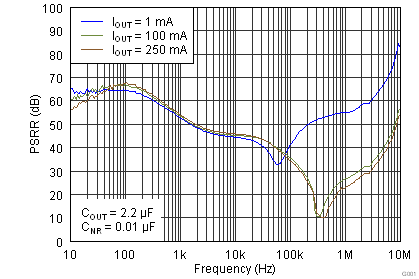 Figure 18. Power-Supply Rejection Ratio vs Frequency
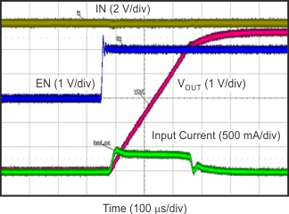 Figure 19. Inrush Current at EN Turn-On
8.3 Do's and Don'ts
Do place at least one 2.2-µF ceramic capacitor as close as possible to the OUT terminal of the regulator.
Do not place the output capacitor more than 10 mm away from the regulator.
Do connect a 0.1-μF to 1.0-μF low equivalent series resistance (ESR) capacitor across the IN terminal and GND input of the regulator.
Do not exceed the absolute maximum ratings.