SLVS887C April 2009 – August 2014 TPS53114
PRODUCTION DATA.
- 1 Features
- 2 Applications
- 3 Description
- 4 Simplified Schematics
- 5 Revision History
- 6 Pin Configurations and Functions
- 7 Specifications
-
8 Detailed Description
- 8.1 Overview
- 8.2 Functional Block Diagram
- 8.3
Feature Description
- 8.3.1 PWM Operation
- 8.3.2 Drivers
- 8.3.3 PWM Frequency and Adaptive On-time Control
- 8.3.4 5-Volt Regulator
- 8.3.5 Soft Start
- 8.3.6 Pre-bias Support
- 8.3.7 Switching Frequency Selection
- 8.3.8 Output Discharge Control
- 8.3.9 Over Current Protection
- 8.3.10 Over/under Voltage Protection
- 8.3.11 UVLO Protection
- 8.3.12 Thermal Shutdown
- 8.4 Device Functional Modes
-
9 Application and Implementation
- 9.1 Application Information
- 9.2
350-kHz Operation Application
- 9.2.1 Design Requirements
- 9.2.2
Detailed Design Procedure
- 9.2.2.1 Choose Inductor
- 9.2.2.2 Choose Output Capacitor
- 9.2.2.3 Choose Input Capacitor
- 9.2.2.4 Choose Bootstrap Capacitor
- 9.2.2.5 Choose VREG5 and V5FILT Capacitors
- 9.2.2.6 Choose Output Voltage Set Point Resistors
- 9.2.2.7 Choose Over Current Set Point Resistor From: IOCL + To: IOCL - minus VOCLoff
- 9.2.2.8 Choose Soft Start Capacitor
- 9.2.2.9 Choose Package Option
- 9.2.3 350 kHz Application Curves
- 9.3 700 kHz Operation Application
- 10Power Supply Recommendations
- 11Layout
- 12Device and Documentation Support
- 13Mechanical, Packaging, and Orderable Information
封装选项
机械数据 (封装 | 引脚)
散热焊盘机械数据 (封装 | 引脚)
- PWP|16
订购信息
1 Features
- D-CAP2™ Mode Control
- High Initial Reference Accuracy (±1%)
- Low Output Ripple
- Wide Input Voltage Range: 4.5 V to 24 V
- Output Voltage Range: 0.76 V to 5.5 V
- Low-Side RDS(on) Loss-Less Current Sensing
- Adaptive Gate Drivers with Integrated Boost Diode
- Adjustable Soft Start
- Pre-Biased Soft Start
- Selectable Switching Frequency
350 kHz / 700 kHz - Cycle-By-Cycle Over Current Limiting Control
- Thermally Compensated OCP by 4000 ppm/°C at ITRIP
2 Applications
- Point-of-Load Regulation in Low Power Systems for Wide Range of Applications
- Digital TV Power Supply
- Networking Home Terminal
- Digital Set Top Box (STB)
- DVD Player / Recorder
- Gaming Consoles
3 Description
The TPS53114 is a single, adaptive on-time D-CAP2™ mode synchronous buck controller. The TPS53114 enables system designers to complete the suite of various end equipment's power bus regulators with cost effective low external component count and low standby current solution. The main control loop for the TPS53114 uses the D-CAP2™ mode control which provides a very fast transient response with no external components. The TPS53114 also has a circuit that enables the device to adapt to both low equivalent series resistance (ESR) output capacitors such as POSCAP or SP-CAP and ultra-low ESR ceramic capacitors. The device provides convenient and efficient operation with input voltages from 4.5 V to 24 V and output voltage from 0.76 V to 5.5 V.
The TPS53114 is available in the 16-pin TSSOP and HTSSOP packages, and is specified from –40°C to 85°C ambient temperature range.
Device Information(1)
| PART NUMBER | PACKAGE | BODY SIZE (NOM) |
|---|---|---|
| TPS53114 | TSSOP (16) | 5.00 mm x 4.40 mm |
| TPS53114 | HTSSOP 916) | 5.00 mm x 4.40 mm |
- For all available packages, see the orderable addendum at the end of the datasheet.
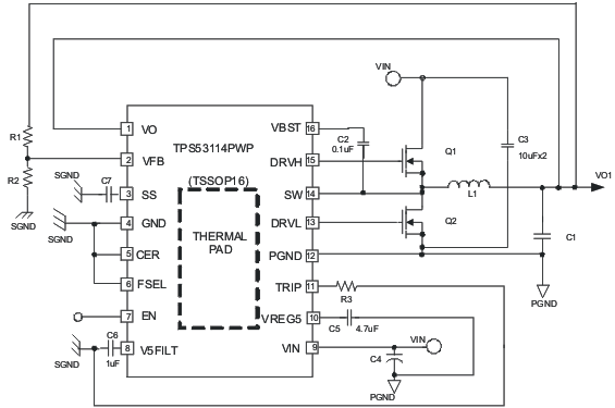
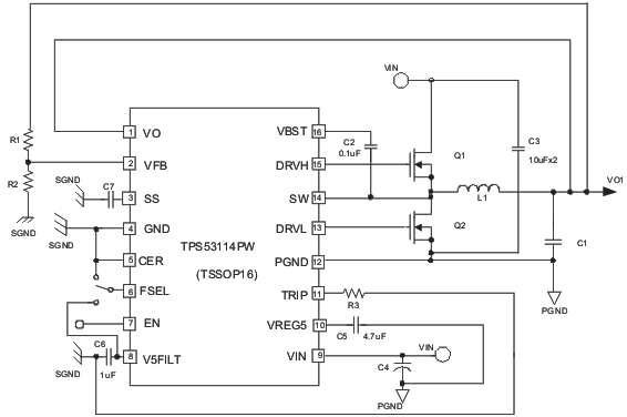
4 Simplified Schematics