SLVS887C April 2009 – August 2014 TPS53114
PRODUCTION DATA.
- 1 Features
- 2 Applications
- 3 Description
- 4 Simplified Schematics
- 5 Revision History
- 6 Pin Configurations and Functions
- 7 Specifications
-
8 Detailed Description
- 8.1 Overview
- 8.2 Functional Block Diagram
- 8.3
Feature Description
- 8.3.1 PWM Operation
- 8.3.2 Drivers
- 8.3.3 PWM Frequency and Adaptive On-time Control
- 8.3.4 5-Volt Regulator
- 8.3.5 Soft Start
- 8.3.6 Pre-bias Support
- 8.3.7 Switching Frequency Selection
- 8.3.8 Output Discharge Control
- 8.3.9 Over Current Protection
- 8.3.10 Over/under Voltage Protection
- 8.3.11 UVLO Protection
- 8.3.12 Thermal Shutdown
- 8.4 Device Functional Modes
-
9 Application and Implementation
- 9.1 Application Information
- 9.2
350-kHz Operation Application
- 9.2.1 Design Requirements
- 9.2.2
Detailed Design Procedure
- 9.2.2.1 Choose Inductor
- 9.2.2.2 Choose Output Capacitor
- 9.2.2.3 Choose Input Capacitor
- 9.2.2.4 Choose Bootstrap Capacitor
- 9.2.2.5 Choose VREG5 and V5FILT Capacitors
- 9.2.2.6 Choose Output Voltage Set Point Resistors
- 9.2.2.7 Choose Over Current Set Point Resistor From: IOCL + To: IOCL - minus VOCLoff
- 9.2.2.8 Choose Soft Start Capacitor
- 9.2.2.9 Choose Package Option
- 9.2.3 350 kHz Application Curves
- 9.3 700 kHz Operation Application
- 10Power Supply Recommendations
- 11Layout
- 12Device and Documentation Support
- 13Mechanical, Packaging, and Orderable Information
封装选项
机械数据 (封装 | 引脚)
散热焊盘机械数据 (封装 | 引脚)
- PWP|16
订购信息
7 Specifications
7.1 Absolute Maximum Ratings
over operating free-air temperature range (unless otherwise noted) (1)| MIN | MAX | UNIT | |||
|---|---|---|---|---|---|
| Input voltage range | VIN, EN | –0.3 | 26 | V | |
| VBST | –0.3 | 32 | |||
| VBST - SW | –0.3 | 6 | |||
| V5FILT, VFB, TRIP, VO, FSEL, CER | –0.3 | 6 | |||
| Output voltage range | DRVH | –1 | 32 | V | |
| DRVH - SW | –0.3 | 6 | |||
| SW | –2 | 26 | |||
| DRVL, VREG5, SS | –0.3 | 6 | |||
| PGND | –0.3 | 0.3 | |||
| TA | Operating ambient temperature range | –40 | 85 | °C | |
| TJ | Junction temperature range | –40 | 150 | °C | |
(1) Stresses beyond those listed under Absolute Maximum Ratings may cause permanent damage to the device. These are stress ratings only, which do not imply functional operation of the device at these or any other conditions beyond those indicated under Recommended Operating Conditions. Exposure to absolute-maximum-rated conditions for extended periods may affect device reliability.
7.2 Handling Ratings
| MIN | MAX | UNIT | |||
|---|---|---|---|---|---|
| Tstg | Storage temperature | –55 | 150 | °C | |
| V(ESD) | Electrostatic discharge | Human body model (HBM), per ANSI/ESDA/JEDEC JS-001, all pins(1) | -2000 | 2000 | V |
| Charged device model (CDM), per JEDEC specification JESD22-C101, all pins(2) | -500 | 500 | |||
(1) JEDEC document JEP155 states that 500-V HBM allows safe manufacturing with a standard ESD control process.
(2) JEDEC document JEP157 states that 250-V CDM allows safe manufacturing with a standard ESD control process.
7.3 Recommended Operating Conditions
over operating free-air temperature range (unless otherwise noted)| MIN | MAX | UNIT | |||
|---|---|---|---|---|---|
| Supply input voltage | VIN | 4.5 | 24 | V | |
| V5FILT | 4.5 | 5.5 | |||
| Input voltage | VBST | –0.1 | 30 | V | |
| VBST - SW | –0.1 | 5.5 | |||
| VFB, VO, FSEL, CER | –0.1 | 5.5 | |||
| TRIP | –0.1 | 0.3 | |||
| EN | –0.1 | 24 | |||
| Output voltage | DRVH | –0.1 | 30 | V | |
| VBST - SW | –0.1 | 5.5 | |||
| SW | 1.8 | 24 | |||
| DRVL, VREG5, SS | –0.1 | 5.5 | |||
| PGND | –0.1 | 0.1 | |||
| TA | Operating free-air temperature | –40 | 85 | °C | |
| TJ | Operating junction temperature | –40 | 125 | °C | |
7.4 Thermal Information
| THERMAL METRIC(1) | TPS53114 | UNIT | ||
|---|---|---|---|---|
| PWP (16 PINS) | PW (16 PINS) | |||
| RθJA | Junction-to-ambient thermal resistance | 51.2 | 109.6 | °C/W |
| RθJC(top) | Junction-to-case (top) thermal resistance | 33.4 | 31.2 | |
| RθJB | Junction-to-board thermal resistance | 28.3 | 54.7 | |
| ψJT | Junction-to-top characterization parameter | 1.4 | 0.9 | |
| ψJB | Junction-to-board characterization parameter | 28.1 | 54.1 | |
| RθJC(bot) | Junction-to-case (bottom) thermal resistance | 4.9 | n/a | |
(1) For more information about traditional and new thermal metrics, see the IC Package Thermal Metrics application report, SPRA953.
7.5 Electrical Characteristics
over operating free-air temperature range (unless otherwise noted)| PARAMETER | TEST CONDITIONS | MIN | TYP | MAX | UNIT | |
|---|---|---|---|---|---|---|
| SUPPLY CURRENT | ||||||
| IIN | VIN supply current | VIN current, TA = 25°C, VREG5 tied to V5FLT, EN = 5V, VFB = 0.8V, SW = 0.5V | 350 | 600 | μA | |
| IVINSDN | VIN shutdown current | VIN current, TA = 25°C, No Load , EN = 0V, VREG5 = ON | 28 | 60 | μA | |
| VFB VOLTAGE and DISCHARGE RESISTANCE | ||||||
| VBG | Bandgap Initial regulation accuracy | TA = 25°C | –1.0% | 1.0% | ||
| VVFBTHL | VFB threshold voltage | TA = 25°C , FSEL = 0 V, CER = V5FILT | 755 | 765 | 775 | mV |
| TA = –40°C to 85°C, FSEL = 0V, CER = V5FILT | 752 | 778 | ||||
| VVFBTHH | VFB threshold voltage | TA = 25°C , FSEL = CER = V5FILT | 748 | 758 | 768 | mV |
| TA = –40°C to 85°C, FSEL = CER = V5FILT | 745 | 771 | ||||
| IVFB | VFB input current | VFB = 0.8V, TA = 25°C | –100 | –10 | 100 | nA |
| RDischg | Vo discharge resistance | EN = 0V, VO = 0.5V, TA = 25°C | 40 | 80 | Ω | |
| VREG5 OUTPUT | ||||||
| VVREG5 | VREG5 output voltage | TA=25°C, 5.5V < VIN < 24V, 0 < IVREG5 < 10mA | 4.6 | 5.0 | 5.2 | V |
| VLN5 | Line regulation | 5.5V < VIN < 24V, IVREG5 = 10mA | 20 | mV | ||
| VLD5 | Load regulation | 1mA < IVREG5 < 10mA | 40 | mV | ||
| IVREG5 | Output current | VIN = 5.5V, VVREG5 = 4.0V, TA = 25°C | 170 | mA | ||
| OUTPUT: N-CHANNEL MOSFET GATE DRIVERS | ||||||
| RDRVH | DRVH resistance | Source, IDRVH = –100mA | 5.5 | 11 | Ω | |
| Sink, IDRVH = 100mA | 2.5 | 5 | ||||
| RDRVL | DRVL resistance | Source, IDRVL = –100mA | 4 | 12 | Ω | |
| Sink, IDRVL = 100mA | 2 | 4 | ||||
| INTERNAL BST DIODE | ||||||
| VFBST | Forward voltage | VVREG5-VBST, IF = 10mA, TA = 25°C | 0.7 | 0.8 | 0.9 | V |
| IVBSTLK | VBST leakage current | VBST = 29V, SW = 24V, TA = 25°C | 0.1 | 1 | µA | |
| SOFT START | ||||||
| Issc | SS charge current | VSS = 0V , SOURCE CURRENT | 1.4 | 2.0 | 2.6 | µA |
| Issd | SS discharge current | VSS = 0.5V , SINK CURRRENT | 100 | 150 | µA | |
| UVLO | ||||||
| VUV5VFILT | V5FILT UVLO threshold | V5FILT rising | 3.7 | 4.0 | 4.3 | V |
| Hysteresis | 0.2 | 0.3 | 0.4 | |||
| LOGIC THRESHOLD | ||||||
| VENH | EN H-level threshold voltage | EN | 2.0 | V | ||
| VENL | EN L-level threshold voltage | EN | 0.3 | V | ||
| CURRENT SENSE | ||||||
| ITRIP | TRIP source current | VTRIP = 0.1V, TA = 25°C | 8.5 | 10 | 11.5 | µA |
| TCITRIP | ITRIP temperature coefficient | on the basis of 25°C | 4000 | ppm/°C | ||
| VOCLoff | OCP compensation offset | (VTRIP-GND-VPGND-SW) voltage, VTRIP-GND = 60mV, TA = 25°C |
–10 | 0 | 10 | mV |
| (VTRIP-GND-VPGND-SW) voltage, VTRIP-GND = 60mV |
–15 | 15 | ||||
| VRtrip | Current limit threshold setting range | VTRIP-GND voltage | 30 | 200 | ||
| OUTPUT UNDERVOLTAGE AND OVERVOLTAGE PROTECTION | ||||||
| VOVP | Output OVP trip threshold | OVP detect | 110% | 115% | 120% | |
| VUVP | Output UVP trip threshold | UVP detect | 65% | 70% | 75% | |
| Hysteresis (recovery <20μs) | 10% | |||||
| THERMAL | ||||||
| TSDN | Thermal shutdown threshold | Shutdown temperature(1) | 150 | °C | ||
| Hysteresis(1) | 20 | |||||
(1) Specified by design. Not production tested.
7.6 Timing Requirements
| PARAMETER | MIN | TYP | MAX | UNIT | ||
|---|---|---|---|---|---|---|
| OUTPUT: N-CHANNEL MOSFET GATE DRIVERS | ||||||
| tD | Dead time | DRVH-low to DRVL-on | 20 | 50 | 80 | ns |
| DRVL-low to DRVH-on | 20 | 40 | 80 | |||
| OUTPUT UNDERVOLTAGE AND OVERVOLTAGE PROTECTION | ||||||
| tOVPDEL | Output OVP prop delay | 1.5 | µs | |||
| tUVPDEL | Output UVP delay | 17 | 30 | 40 | µs | |
| tUVPEN | Output UVP enable delay | UVP enable delay / soft start time | X1.4 | X1.7 | X2.0 | |
7.7 Switching Characteristics
over operating free-air temperature range (unless otherwise noted)| PARAMETER | TEST CONDITIONS | MIN | TYP | MAX | UNIT | |
|---|---|---|---|---|---|---|
| ON-TIME TIMER CONTROL | ||||||
| tONL | On time | SW = 12V, VO = 1.8V, FSEL = 0V | 390 | ns | ||
| tONH | On time | SW = 12V, VO = 1.8V, FSEL = V5FILT | 139 | ns | ||
| tOFFL | Min off time | SW = 0.7V, TA = 25°C, VFB = 0.7V, FSEL = 0V | 285 | ns | ||
| tOFFH | Min off time | SW = 0.7V, TA = 25°C, VFB = 0.7V, FSEL = V5FILT | 216 | ns | ||
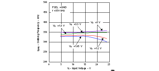
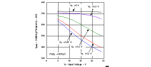
7.8 Typical Characteristics
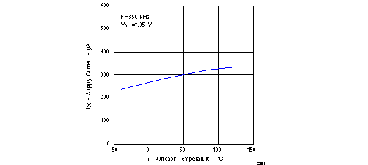
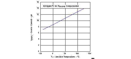
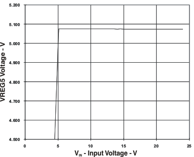
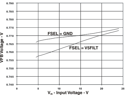
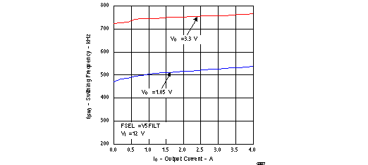
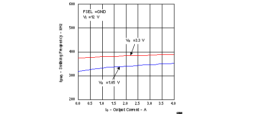 Figure 9. Switching Frequency vs. Output Current