SLVS887C April 2009 – August 2014 TPS53114
PRODUCTION DATA.
- 1 Features
- 2 Applications
- 3 Description
- 4 Simplified Schematics
- 5 Revision History
- 6 Pin Configurations and Functions
- 7 Specifications
-
8 Detailed Description
- 8.1 Overview
- 8.2 Functional Block Diagram
- 8.3
Feature Description
- 8.3.1 PWM Operation
- 8.3.2 Drivers
- 8.3.3 PWM Frequency and Adaptive On-time Control
- 8.3.4 5-Volt Regulator
- 8.3.5 Soft Start
- 8.3.6 Pre-bias Support
- 8.3.7 Switching Frequency Selection
- 8.3.8 Output Discharge Control
- 8.3.9 Over Current Protection
- 8.3.10 Over/under Voltage Protection
- 8.3.11 UVLO Protection
- 8.3.12 Thermal Shutdown
- 8.4 Device Functional Modes
-
9 Application and Implementation
- 9.1 Application Information
- 9.2
350-kHz Operation Application
- 9.2.1 Design Requirements
- 9.2.2
Detailed Design Procedure
- 9.2.2.1 Choose Inductor
- 9.2.2.2 Choose Output Capacitor
- 9.2.2.3 Choose Input Capacitor
- 9.2.2.4 Choose Bootstrap Capacitor
- 9.2.2.5 Choose VREG5 and V5FILT Capacitors
- 9.2.2.6 Choose Output Voltage Set Point Resistors
- 9.2.2.7 Choose Over Current Set Point Resistor From: IOCL + To: IOCL - minus VOCLoff
- 9.2.2.8 Choose Soft Start Capacitor
- 9.2.2.9 Choose Package Option
- 9.2.3 350 kHz Application Curves
- 9.3 700 kHz Operation Application
- 10Power Supply Recommendations
- 11Layout
- 12Device and Documentation Support
- 13Mechanical, Packaging, and Orderable Information
封装选项
机械数据 (封装 | 引脚)
散热焊盘机械数据 (封装 | 引脚)
- PWP|16
订购信息
11 Layout
11.1 Layout Guidelines
- Keep the input switching current loop as small as possible.
- Place the input capacitor (C3) close to the top switching FET.
- Place the input capacitor (C4) close to the IC VIN pin.
- The output current loop should also be kept as small as possible.
- Keep the SW node as physically small and short as possible as to minimize parasitic capacitance and inductance and to minimize radiated emissions.
- Independent connections should be brought from the output to the feedback pin (VFB) and VO pin of the device.
- Keep analog and non-switching components away from switching components.
- Terminate the feedback resistor divider (R2), slow start capacitor C7), CER pin, V5FILT capacitor (C6) and TRIP resistor (R3) to signal ground (SGND).
- Connect the signal ground (SGND) copper area to the GND pin at the GND pin.
- Make a single point connection from the signal ground to power ground directly under the IC as shown.
- Do not allow switching current to flow under the device.
11.2 Layout Example
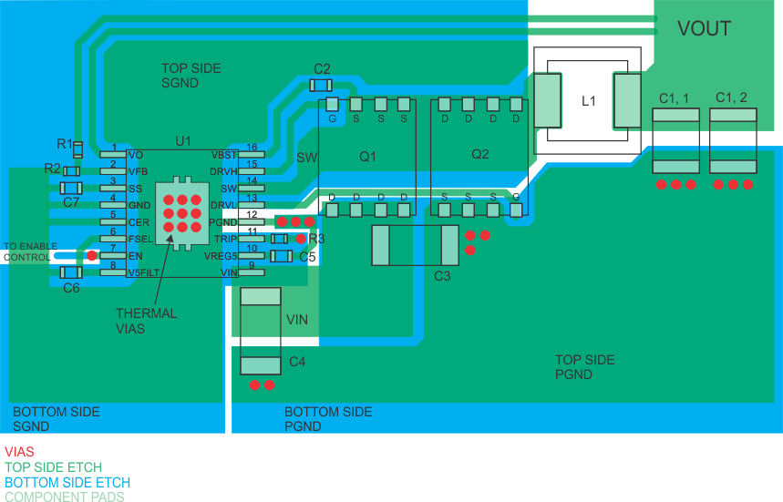 Figure 22. Typical TPS53114 Layout