SLVS887C April 2009 – August 2014 TPS53114
PRODUCTION DATA.
- 1 Features
- 2 Applications
- 3 Description
- 4 Simplified Schematics
- 5 Revision History
- 6 Pin Configurations and Functions
- 7 Specifications
-
8 Detailed Description
- 8.1 Overview
- 8.2 Functional Block Diagram
- 8.3
Feature Description
- 8.3.1 PWM Operation
- 8.3.2 Drivers
- 8.3.3 PWM Frequency and Adaptive On-time Control
- 8.3.4 5-Volt Regulator
- 8.3.5 Soft Start
- 8.3.6 Pre-bias Support
- 8.3.7 Switching Frequency Selection
- 8.3.8 Output Discharge Control
- 8.3.9 Over Current Protection
- 8.3.10 Over/under Voltage Protection
- 8.3.11 UVLO Protection
- 8.3.12 Thermal Shutdown
- 8.4 Device Functional Modes
-
9 Application and Implementation
- 9.1 Application Information
- 9.2
350-kHz Operation Application
- 9.2.1 Design Requirements
- 9.2.2
Detailed Design Procedure
- 9.2.2.1 Choose Inductor
- 9.2.2.2 Choose Output Capacitor
- 9.2.2.3 Choose Input Capacitor
- 9.2.2.4 Choose Bootstrap Capacitor
- 9.2.2.5 Choose VREG5 and V5FILT Capacitors
- 9.2.2.6 Choose Output Voltage Set Point Resistors
- 9.2.2.7 Choose Over Current Set Point Resistor From: IOCL + To: IOCL - minus VOCLoff
- 9.2.2.8 Choose Soft Start Capacitor
- 9.2.2.9 Choose Package Option
- 9.2.3 350 kHz Application Curves
- 9.3 700 kHz Operation Application
- 10Power Supply Recommendations
- 11Layout
- 12Device and Documentation Support
- 13Mechanical, Packaging, and Orderable Information
封装选项
机械数据 (封装 | 引脚)
散热焊盘机械数据 (封装 | 引脚)
- PWP|16
订购信息
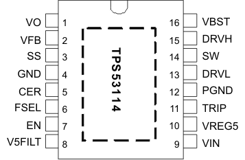
6 Pin Configurations and Functions
16-Pin HTSSOP
PWP Package
(Top View)
16-Pin TSSOP
PW Package
(Top View)
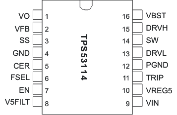
Pin Functions
| PIN | I/O | DESCRIPTION | |
|---|---|---|---|
| NAME | NUMBER | ||
| VBST | 16 | I | Supply input for high-side NFET driver. Bypass to SW with a high-quality 0.1-μF ceramic capacitor. An external schottky diode can be added from VREG5 if forward drop is critical to drive the high-side FET. |
| EN | 7 | I | Enable. Pull High to enable SMPS. |
| SS | 3 | O | Soft start programming pin. Connect capacitor from SS pin to GND to program soft start time. |
| VO | 1 | I | Output voltage input for on-time adjustment and output discharge. Connect directory to the output voltage. |
| VFB | 2 | I | D-CAP2 feedback input. Connect to output voltage with resistor divider. |
| GND | 4 | I | Signal ground pin. Connect to PGND and system ground at a single point. |
| DRVH | 15 | O | High-side N-channel MOSFET gate driver output. SW referenced driver switches between SW(OFF) and VBST(ON). |
| SW | 14 | I/O | Switch node connections for both the high-side driver and over current comparator. |
| DRVL | 13 | O | Low-side N-Channel MOSFET gate driver output. PGND referenced driver switches between PGND(OFF) and VREG5(ON). |
| PGND | 12 | I/O | Power ground connection for both the low-side driver and over current comparator. Connect PGND and GND strongly together near the IC. |
| TRIP | 11 | I | over current threshold programming pin. Connect to GND with a resister to set threshold for low-side RDS(on) current limit. |
| VIN | 9 | I | Supply Input for 5-V linear regulator. Bypass to GND with a minimum high-quality 0.1-μF ceramic capacitor. |
| V5FILT | 8 | I | 5-V supply input for the control circuitry except the MOSFET drivers. Bypass to GND with a minimum high-quality 1.0-μF ceramic capacitor. V5FILT is connected to VREG5 via internal 10-Ω resistor. |
| VREG5 | 10 | O | Output of 5-V linear regulator and supply for MOSFET driver. Bypass to GND with a minimum high-quality 4.7-μF ceramic capacitor. VREG5 is connected to V5FILT via internal 10-Ω resistor. |
| CER | 5 | I | Output capacitor select pin. Connect to GND for ceramic output capacitors. Connect to V5FILT for conductive polymer electrolyte type output capacitors (SP-CAP, POS-CAP, PXE). |
| FSEL | 6 | I | Switching frequency selection pin. Connect to GND for low switching frequency or connect to V5FILT for high switching frequency. |