ZHCS179F August   2011  – July 2016

PRODUCTION DATA.  

  1. 特性
  2. 应用
  3. 说明
  4. 修订历史记录
  5. Device Comparison Table
  6. Pin Configuration and Functions
  7. Specifications
    1. 7.1 Absolute Maximum Ratings
    2. 7.2 ESD Ratings
    3. 7.3 Recommended Operating Conditions
    4. 7.4 Thermal Information
    5. 7.5 Electrical Characteristics
    6. 7.6 Typical Characteristics
  8. Detailed Description
    1. 8.1 Overview
    2. 8.2 Functional Block Diagram
    3. 8.3 Feature Description
      1. 8.3.1  Inside the INA826
      2. 8.3.2  Setting the Gain
        1. 8.3.2.1 Gain Drift
      3. 8.3.3  Offset Trimming
      4. 8.3.4  Input Common-Mode Range
      5. 8.3.5  Input Protection
      6. 8.3.6  Input Bias Current Return Path
      7. 8.3.7  Reference Terminal
      8. 8.3.8  Dynamic Performance
      9. 8.3.9  Operating Voltage
        1. 8.3.9.1 Low-Voltage Operation
      10. 8.3.10 Error Sources
    4. 8.4 Device Functional Modes
  9. Application and Implementation
    1. 9.1 Application Information
    2. 9.2 Typical Application
      1. 9.2.1 Design Requirements
      2. 9.2.2 Detailed Design Procedure
      3. 9.2.3 Application Curves
    3. 9.3 System Examples
      1. 9.3.1 Circuit Breaker
      2. 9.3.2 Programmable Logic Controller (PLC) Input
      3. 9.3.3 Using TINA-TI SPICE-Based Analog Simulation Program with the INA826
  10. 10Power Supply Recommendations
  11. 11Layout
    1. 11.1 Layout Guidelines
      1. 11.1.1 CMRR vs Frequency
    2. 11.2 Layout Example
  12. 12器件和文档支持
    1. 12.1 文档支持
      1. 12.1.1 相关文档
    2. 12.2 接收文档更新通知
    3. 12.3 社区资源
    4. 12.4 商标
    5. 12.5 静电放电警告
    6. 12.6 Glossary
  13. 13机械、封装和可订购信息

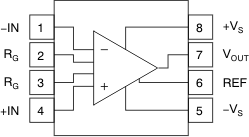
Pin Configuration and Functions

DGK and D Package
8-Pin SOIC, VSSOP
Top View
INA826 po_bos562.gif
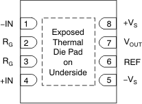
DRG Package
8-Pin WSON
Top View
INA826 po_dfn_bos562.gif

Pin Functions

PIN I/O DESCRIPTION
NAME NO.
SOIC, VSSOP WSON
–IN 1 1 I Negative (inverting) input
+IN 4 4 I Positive (noninverting) input
REF 6 6 I Reference input. This pin must be driven by low impedance.
RG 2 2 Gain setting pin. Place a gain resistor between pin 2 and pin 3.
3 3
VOUT 7 7 O Output
–VS 5 5 Negative supply
+VS 8 8 Positive supply