ZHCS179F August 2011 – July 2016
PRODUCTION DATA.
- 1 特性
- 2 应用
- 3 说明
- 4 修订历史记录
- 5 Device Comparison Table
- 6 Pin Configuration and Functions
- 7 Specifications
-
8 Detailed Description
- 8.1 Overview
- 8.2 Functional Block Diagram
- 8.3 Feature Description
- 8.4 Device Functional Modes
- 9 Application and Implementation
- 10Power Supply Recommendations
- 11Layout
- 12器件和文档支持
- 13机械、封装和可订购信息
9 Application and Implementation
NOTE
Information in the following applications sections is not part of the TI component specification, and TI does not warrant its accuracy or completeness. TI’s customers are responsible for determining suitability of components for their purposes. Customers should validate and test their design implementation to confirm system functionality.
9.1 Application Information
The low power consumption, high performance, and low cost of the INA826 make the device an excellent instrumentation amplifier for many applications. The INA826 can be used in many low-power, portable applications because the device has a low quiescent current (200 µA, typ) and comes in a small 8-pin WSON package. The input protection circuitry, low maximum gain drift, low offset voltage, and 36-V maximum supply voltage also make the INA826 an ideal choice for industrial applications as well.
9.2 Typical Application
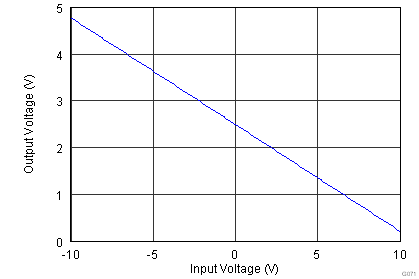
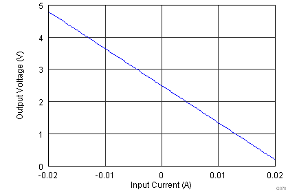
Figure 63 shows a three-terminal programmable-logic controller (PLC) design for the INA826. This PLC reference design accepts inputs of ±10 V or ±20 mA. The output is a single-ended voltage of 2.5 V ±2.3 V (or 200 mV to 4.8 V). Many PLCs typically have these input and output ranges.
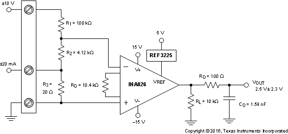 Figure 63. Three-Terminal PLC Design
9.2.1 Design Requirements
This design has these requirements:
- Supply voltage: ±15 V, 5 V
- Inputs: ±10 V, ±20 mA
- Output: 2.5 V, ±2.3 V
9.2.2 Detailed Design Procedure
There are two modes of operation for the circuit shown in Figure 63: current input and voltage input. This design requires R1 >> R2 >> R3. Given this relationship, the current input mode transfer function is given by Equation 2.

where
- G represents the gain of the instrumentation amplifier
The transfer function for the voltage input mode is shown by Equation 3.

R1 sets the input impedance of the voltage input mode. The minimum typical input impedance is 100 kΩ. 100 kΩ is selected for R1 because increasing the R1 value also increases noise. The value of R3 must be extremely small compared to R1 and R2. 20 Ω for R3 is selected because that resistance value is much smaller than R1 and yields an input voltage of ±400 mV when operated in current mode (±20 mA).
Equation 4 can be used to calculate R2 given VD = ±400 mV, VIN = ±10 V, and R1 = 100 kΩ.

The value obtained from Equation 4 is not a standard 0.1% value, so 4.12 kΩ is selected. R1 and R2 also use 0.1% tolerance resistors to minimize error.
The ideal gain of the instrumentation amplifier is calculated with Equation 5.

Using the INA826 gain equation, the gain-setting resistor value is calculated as shown by Equation 6.

10.4 kΩ is a standard 0.1% resistor value that can be used in this design. Finally, the output RC filter components are selected to have a –3-dB cutoff frequency of 1 MHz.
9.3 System Examples
9.3.1 Circuit Breaker
Figure 66 shows the INA826 used in a circuit breaker application.
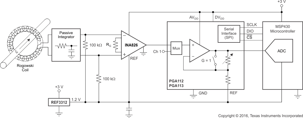 Figure 66. Circuit Breaker Example
9.3.2 Programmable Logic Controller (PLC) Input
The INA826 used in an example programmable logic controller (PLC) input application is shown in Figure 67.
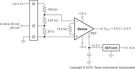 Figure 67. ±10-V, 4-mA to 20-mA PLC Input
Additional application ideas are illustrated in Figure 68 to Figure 72.
9.3.3 Using TINA-TI SPICE-Based Analog Simulation Program with the INA826
TINA is a simple, powerful, and easy-to-use circuit simulation program based on a SPICE engine. TINA-TI is a free, fully-functional version of the TINA software, preloaded with a library of macromodels in addition to a range of both passive and active models. TINA provides all the conventional dc, transient, and frequency domain analysis of SPICE as well as additional design capabilities.
Available as a free download from the Analog eLab Design Center, TINA-TI offers extensive post-processing capability that allows users to format results in a variety of ways. Virtual instruments offer users the ability to select input waveforms and probe circuit nodes, voltages, and waveforms, creating a dynamic quick-start tool.
Figure 68 and Figure 70 illustrate example TINA-TI circuits for the INA826 that can be used to develop, modify, and assess the circuit design for specific applications. Links to download these simulation files are provided in this section.
NOTE
These files require that either the TINA software (from DesignSoft) or TINA-TI software be installed. Download the free TINA-TI software from the TINA-TI folder.
The circuit in Figure 68 is used to convert inputs of ±10 V, ±5 V, or ±20 mA to an output voltage range from 0.5 V to 4.5 V. The input selection depends on the settings of SW1 and SW2. Further explanation as well as the TINA-TI simulation circuit is provided in the compressed file that can be downloaded at the following link: PLC Circuit.
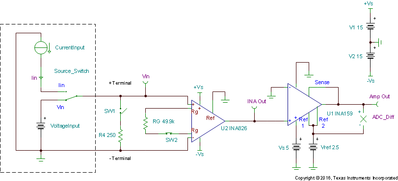 Figure 68. Two-Terminal Programmable Logic Controller (PLC) Input
Figure 69 is an example of a LEAD I ECG circuit. The input signals come from leads attached to the right arm (RA) and left arm (LA). These signals are simulated with the circuitry in the corresponding boxes. Protection resistors (RPROT1 and RPROT2) and filtering are also provided. The OPA333 is used as an integrator to remove the gained-up dc offsets and servo the INA826 outputs to VREF. Finally, the right leg drive is biased to a potential (+VS / 2) and inverts and amplifies the average common-mode signal back into the patient's right leg. This architecture reduces the 50- and 60-Hz noise pickup.
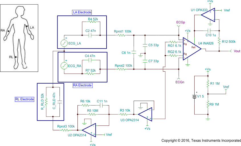 Figure 69. ECG Circuit
Figure 70 shows an example of how the INA826 can be used for low-side current sensing. The load current (ILOAD) creates a voltage drop across the shunt resistor (RSHUNT). This voltage is amplified by the INA826 with gain set to 100. The output swing of the INA826 is set by the common-mode voltage (which is 0 V in low-side current sensing) and power supplies. Therefore, a dual-supply circuit is implemented. The load current is set from 1 A to 10 A, corresponding to an output voltage range from 350 mV to 3.5 V. The output range can be adjusted by changing the shunt resistor and the gain of the INA826. Click the following link to download the TINA-TI file: Current Sensing Circuit.
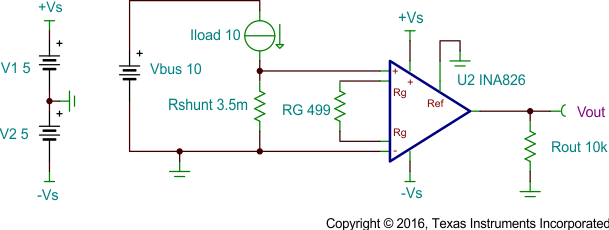 Figure 70. Low-Side Current Sensing
Figure 71 shows an example of how the INA826 can be used for RTD signal conditioning. This circuit creates an excitation current (ISET) by forcing 2.5 V from the REF5025 across RSET. The zero-drift, low-noise OPA188 creates the virtual ground that maintains a constant differential voltage across RSET with changing common-mode voltage. This voltage is necessary because the voltage on the positive input of the INA826 fluctuates over temperature as a result of the changing RTD resistance. Click the following link to download the TINA-TI file: RTD Circuit.
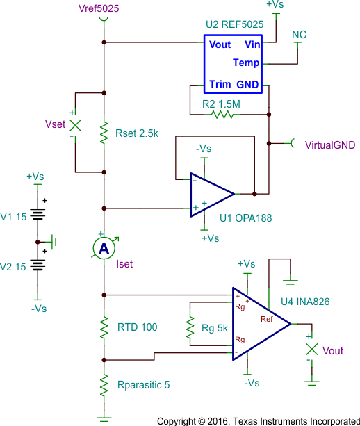 Figure 71. RTD Signal Conditioning
The circuit in Figure 72 creates a precision current ISET by forcing the INA826 VDIFF across RSET. The input voltage VIN is amplified to the output of the INA826 and then divided down by the gain of the INA826 to create VDIFF. ISET can be controlled either by changing the value of the gain-set resistor RG, the set resistor RSET, or by changing VOUT through the gain of the composite loop. Care must be taken to ensure that the changing load resistance RL does not create a voltage on the negative input of the INA826 that violates the compliance of the common-mode input range. Likewise, the voltage on the output of the OPA170 must remain compliant throughout the changing load resistance for this circuit to function properly.
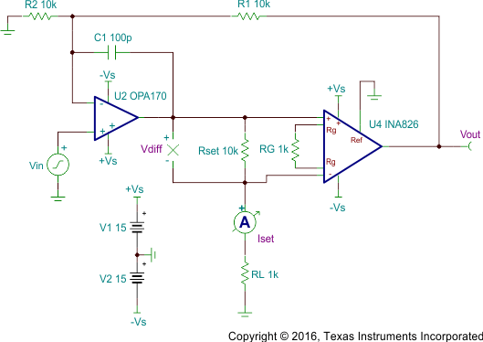 Figure 72. Precision Current Source
