ZHCS179F August 2011 – July 2016
PRODUCTION DATA.
- 1 特性
- 2 应用
- 3 说明
- 4 修订历史记录
- 5 Device Comparison Table
- 6 Pin Configuration and Functions
- 7 Specifications
-
8 Detailed Description
- 8.1 Overview
- 8.2 Functional Block Diagram
- 8.3 Feature Description
- 8.4 Device Functional Modes
- 9 Application and Implementation
- 10Power Supply Recommendations
- 11Layout
- 12器件和文档支持
- 13机械、封装和可订购信息
11 Layout
11.1 Layout Guidelines
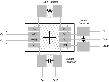
Attention to good layout practices is always recommended. Keep traces short and, when possible, use a printed circuit board (PCB) ground plane with surface-mount components placed as close to the device pins as possible. Place 0.1-μF bypass capacitors close to the supply pins. Apply these guidelines throughout the analog circuit to improve performance and provide benefits such as reducing the electromagnetic-interference (EMI) susceptibility.
The INA826EVM is intended to provide basic functional evaluation of the INA826. An image of the INA826EVM is provided in Figure 73. The INA826EVM is also available for purchase through the TI eStore.
11.1.1 CMRR vs Frequency
The INA826 pinout is optimized for achieving maximum CMRR performance over a wide range of frequencies. However, care must be taken to ensure that both input paths are well-matched for source impedance and capacitance to avoid converting common-mode signals into differential signals. In addition, parasitic capacitance at the gain-setting pins can also affect CMRR over frequency. For example, in applications that implement gain switching using switches or PhotoMOS® relays to change the value of RG, choose the component so that the switch capacitance is as small as possible.
11.2 Layout Example
 Figure 73. INA826 Example Layout
The INA826EVM provides the following features:
- Intuitive evaluation with silkscreen schematic
- Easy access to nodes with surface-mount test points
- Advanced evaluation with two prototype areas
- Reference voltage source flexibility
- Convenient input and output filtering