SLVS813C June 2008 – November 2016 UCD9081
PRODUCTION DATA.
- 1 Features
- 2 Applications
- 3 Description
- 4 Revision History
- 5 Pin Configuration and Functions
- 6 Specifications
- 7 Parameter Measurement Information
-
8 Detailed Description
- 8.1 Overview
- 8.2 Functional Block Diagram
- 8.3 Feature Description
- 8.4 Device Functional Modes
- 8.5 Programming
- 8.6 Register Maps
- 9 Application and Implementation
- 10Power Supply Recommendations
- 11Layout
- 12Device and Documentation Support
- 13Mechanical, Packaging, and Orderable Information
6 Specifications
6.1 Absolute Maximum Ratings
over operating free-air temperature range (unless otherwise noted)(1)| MIN | MAX | UNIT | |
|---|---|---|---|
| Voltage applied from VCC to VSS | –0.3 | 4.1 | V |
| Voltage applied to any pin(2) | –0.3 | VCC + 0.3 | V |
| ESD diode current at any device terminal | ±2 | mA | |
| Storage temperature, Tstg | –40 | 85 | °C |
(1) Stresses beyond those listed under Absolute Maximum Ratings may cause permanent damage to the device. These are stress ratings only, which do not imply functional operation of the device at these or any other conditions beyond those indicated under Recommended Operating Conditions. Exposure to absolute-maximum-rated conditions for extended periods may affect device reliability.
(2) All voltages referenced to VSS.
6.2 Recommended Operating Conditions
| MIN | NOM | MAX | UNIT | ||
|---|---|---|---|---|---|
| VCC | Supply voltage during operation and configuration changes | 3 | 3.3 | 3.6 | V |
| TA | Operating free-air temperature | –40 | 85 | °C | |
6.3 Thermal Information
| THERMAL METRIC(1) | UCD9081 | UNIT | |
|---|---|---|---|
| RHB (VQFN) | |||
| 32 PINS | |||
| RθJA | Junction-to-ambient thermal resistance | 32.1 | °C/W |
| RθJC(top) | Junction-to-case (top) thermal resistance | 18.1 | °C/W |
| RθJB | Junction-to-board thermal resistance | 6 | °C/W |
| ψJT | Junction-to-top characterization parameter | 0.2 | °C/W |
| ψJB | Junction-to-board characterization parameter | 5.9 | °C/W |
| RθJC(bot) | Junction-to-case (bottom) thermal resistance | 1.2 | °C/W |
(1) For more information about traditional and new thermal metrics, see the Semiconductor and IC Package Thermal Metrics application report.
6.4 Electrical Characteristics
These specifications are over recommended ranges of supply voltage and operating free-air temperature (unless otherwise noted)| PARAMETER | TEST CONDITIONS | MIN | TYP | MAX | UNIT | ||
|---|---|---|---|---|---|---|---|
| SUPPLY CURRENT | |||||||
| IS | Supply current into VCC | TA = 25°C, excluding external current | 3 | 4 | mA | ||
| IC | Supply current during configuration | VCC = 3.6 V | 3 | 7 | mA | ||
| STANDARD INPUTS (RST, TEST) | |||||||
| VIL | Low-level input voltage | VCC = 3 V | VSS | VSS + 0.6 | V | ||
| VIH | High-level input voltage | VCC = 3 V | 0.8 × VCC | VCC | V | ||
| SCHMITT TRIGGER INPUTS (SDA, SCL, EN[1...7], EN8/ADDR1, ADDR[2...4]) | |||||||
| VIT+ | Positive-going input threshold voltage | VCC = 3 V | 1.5 | 1.9 | V | ||
| VIT– | Negative-going input threshold voltage | VCC = 3 V | 0.9 | 1.3 | V | ||
| Vhys | Input voltage hysteresis | VCC = 3 V, VIT+ – VIT– | 0.5 | 1 | V | ||
| Ilkg | High-impedance leakage current | ±50 | nA | ||||
| ANALOG INPUTS (MONx, ROSC) | |||||||
| VCC | Analog supply voltage | VSS = 0 V | 3 | 3.6 | V | ||
| VMON<1..8> | Analog input voltage | Internal voltage reference selected | 0 | 2.5 | V | ||
| External voltage reference selected (VCC used as reference) |
0 | VCC | |||||
| CI(1) | Input capacitance | Only one terminal can be selected at a time (MON1 to MON8) | 27 | pF | |||
| RI(1) | Input MUX ON resistance | 0 V ≤ VMONx ≤ VCC, VCC = 3 V | 2000 | Ω | |||
| Ilkg | High-impedance leakage current | MON1 to MON8 | ±50 | nA | |||
| VREF+ | Positive internal reference voltage | Internal voltage reference selected, VCC = 3 V |
2.35 | 2.5 | 2.65 | V | |
| VTUE | ADC total unadjusted error | VCC = 3 V | VR+ = 2.5 V (internal reference) |
±12.2 | mV | ||
| VR+ = VCC
(external reference) |
±14.7 | ||||||
| TREF+(1) | Temperature coefficient of internal voltage reference | I(VREF+) is a constant in the range of 0 mA ≤ I(VREF+) ≤ 1 mA, VCC = 3 V |
±100 | ppm/°C | |||
| MISCELLANEOUS | |||||||
| Tretention | Retention of configuration parameters | TJ = 25°C | 100 | Years | |||
| POR, BROWNOUT, RESET(4)(5) | |||||||
| td(BOR) | Brownout | 2000 | µs | ||||
| VCC(start) | Brownout | dVCC/dt ≤ 3 V/s | 0.7 × V(B_IT–) | V | |||
| V(B_IT–) | Brownout | dVCC/dt ≤ 3 V/s | 1.71 | V | |||
| Vhys(B_IT–) | Brownout | dVCC/dt ≤ 3 V/s | 70 | 130 | 180 | mV | |
| t(reset) | Brownout | Pulse length required at RST pin to accept reset internally, VCC = 3 V | 2 | µs | |||
| DIGITAL OUTPUTS (EN8/GPO1, GPO[2...4], EN[1...7], SDA, SCL) | |||||||
| VOH | High-level output voltage | IOHmax = –1.5 mA(2), VCC = 3 V | VCC – 0.25 | VCC | V | ||
| IOHmax = –6 mA(3), VCC = 3 V | VCC – 0.6 | VCC | |||||
| VOL | Low-level output voltage | IOLmax = 1.5 mA(2), VCC = 3 V | VSS | VSS + 0.25 | V | ||
| IOLmax = 6 mA(3), VCC = 3 V | VSS | VSS + 0.6 | |||||
| Ilkg | High-impedance leakage current | VCC = 3 V | ±50 | nA | |||
(1) Not production tested. Limits verified by design.
(2) The maximum total current, IOHmax and IOLmax, for all outputs combined, must not exceed ±12 mA to hold the maximum voltage drop specified.
(3) The maximum total current, IOHmax and IOLmax, for all outputs combined, must not exceed ±48 mA to hold the maximum voltage drop specified.
(4) The current consumption of the brown-out module is already included in the ICC current consumption data.
(5) During power up, device initialization starts following a period of td(BOR) after VCC = V(B_IT–) + Vhys(B_IT–).
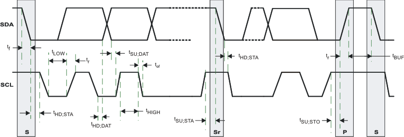
6.5 Timing Requirements: I2C Interface
| MIN | MAX | UNIT | ||
|---|---|---|---|---|
| tofof | Output fall time from VOH to VOL(1) with a bus capacitance from 10 pF to 400 pF | 250(2) | ns | |
| CI | Capacitance for each pin | 10 | pF | |
| fSCL | SCL clock frequency | 10 | 100 | kHz |
| tHD;STA | Repeated hold time START condition (after this period, the first clock pulse is generated) | 4 | µs | |
| tHD;DAT | Data hold time | 0(3) | 3.45(4) | µs |
| tLOW | LOW period of the SCL clock | 4.7 | µs | |
| tHIGH | HIGH period of the SCL clock | 4 | µs | |
| tSU;STA | Setup time for repeated start condition | 4.7 | µs | |
| tSU;DAT | Data setup time | 250 | ns | |
| tr | Rise time of both SDA and SCL signals | 1000 | ns | |
| tf | Fall time of both SDA and SCL signals | 300 | ns | |
| tSU;STO | Setup time for STOP condition | 4 | µs | |
| tBUF | Bus free time between a STOP and START condition | 4.7 | µs | |
| C(b) | Capacitive load for each bus line | 400 | pF | |
| VnL | Noise margin at the LOW level for each connected device (including hysteresis) | 0.1 × VDD | V | |
| VnH | Noise margin at the HIGH level for each connected device (including hysteresis) | 0.2 × VDD | V | |
(1) See Electrical Characteristics
(2) The maximum tf for the SDA and SCL bus lines (300 ns) is longer than the specified maximum tof for the output stages (250 ns). This allows series protection resistors, Rs , to be connected between the SDA/SCL pins and the SDA/SCL bus lines without exceeding the maximum specified tf.
(3) A device must internally provide a hold time of at least 300 ns for the SDA signal to bridge the undefined region of the falling edge of SCL.
(4) The maximum tHD;DAT must only be met if the device does not stretch the LOW period (tLOW) of the SCL signal.
 Figure 1. Timing Diagram for I2C Interface
6.6 Typical Characteristics
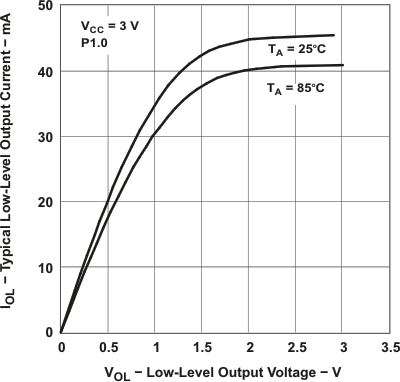
Digital outputs (only one output is loaded at a time) Figure 2. Typical Low-Level Output Current
vs Low-Level Output Voltage
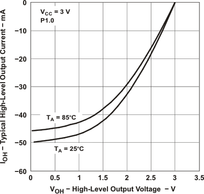
 Figure 3. Typical High-Level Output Current
vs High-Level Output Voltage