SLVS813C June 2008 – November 2016 UCD9081
PRODUCTION DATA.
- 1 Features
- 2 Applications
- 3 Description
- 4 Revision History
- 5 Pin Configuration and Functions
- 6 Specifications
- 7 Parameter Measurement Information
-
8 Detailed Description
- 8.1 Overview
- 8.2 Functional Block Diagram
- 8.3 Feature Description
- 8.4 Device Functional Modes
- 8.5 Programming
- 8.6 Register Maps
- 9 Application and Implementation
- 10Power Supply Recommendations
- 11Layout
- 12Device and Documentation Support
- 13Mechanical, Packaging, and Orderable Information
8 Detailed Description
8.1 Overview
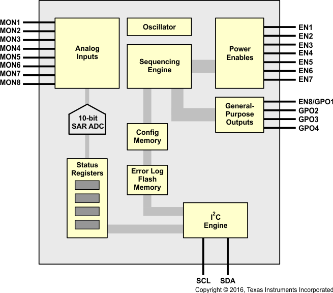
Electronic systems that include CPU, DSP, microcontroller, FPGA, ASIC, and so forth, can have multiple voltage rails and require certain power on and off sequences to function correctly. The UCD9081 device can control up to 8 voltage rails and ensure correct power sequences during normal condition and fault conditions.
In addition to sequencing, UCD9081 can continuously monitor rail voltages, fault conditions, and report the system health information to a I2C host, improving the long-term reliability of the system.
Also, UCD9081 can protect electronic systems by responding to power system faults. The fault responses are conveniently configured by users through PC-based GUI. Fault events are stored in on-chip nonvolatile flash memory to assist failure analysis.
The UCD9081 can control up to four general-purpose digital outputs through the same sequencing mechanisms as the power supply enables, which can be used for digital signals for other devices.
8.2 Functional Block Diagram
8.3 Feature Description
8.3.1 Rail Configuration
A rail includes voltage monitoring pin, a power-supply enable. UCD9081 can support up to 8 rails. Once the assigned rail is selected, other key monitoring and sequencing criteria are selected for each rail from rail configuration:
- Enable pin polarity
- Undervoltage (UV) and overvoltage (OV) fault limits
- Maximum time allowed before an alarm is declared
- Maximum time allowed achieving regulation (voltage between UV or OV range)
- Masks glitches from error log windows
- Log errors to flash
- Sequence after shutdown
- Voltage divider
- Sequence conditions selections
- Alarm actions
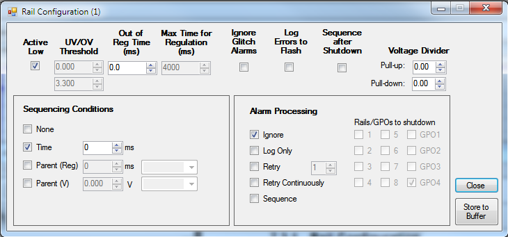 Figure 7. GUI Rail Configuration
8.3.2 Graphical User Interface (GUI)
UCD9081 designer is provided for device configuration. This PC-based graphical user interface (GUI) offers an intuitive I2C interface to the device. It allows the design engineer to configure the system operating parameters for the application without directly using I2C commands, store the configuration to on-chip nonvolatile memory, and observe system status (voltage, and so forth). The UCD9081 GUI can be downloaded from www.ti.com in the product folder.
8.4 Device Functional Modes
8.4.1 Power Supply Sequencing
The UCD9081 can be configured to sequence power supply rails using the enable signals (ENx) or the general-purpose outputs (GPOx) in one of four ways:
- A rail can be configured to not be sequenced
- Using a delay time after UCD9081 RESET. The enable or GPO is asserted after UCD9081 RESET plus the user specified delay
- Using a delay time after another (parent) rail has achieved regulation (VRAIL is within specified under- and overvoltage settings). The enable or GPO is asserted after the (parent) rail is in regulation plus the user specified delay.
- Using a (parent) rail voltage. The enable or GPO is asserted after the (parent) rail voltage is greater than or equal to the user specified voltage.
8.4.2 Power-Supply Enables
The UCD9081 can sequence and enable or disable up to eight power supplies through the ENx (EN1 to EN8) signals. These signals can be configured active-high or active-low, supporting power supplies with either polarity.
EN8 can also be configured as a GPO (GPO1). EN8/ADDR1/GPO1 is also used for I2C address selection (ADDR1).
While the UCD9081 is in RESET, the enable signals are in a high-impedance state. The enable signals must be pulled up or down on the board according to the desired default power-supply state (enabled or disabled).
8.4.3 General-Purpose Outputs
The UCD9081 can control up to four general-purpose digital outputs through the same sequencing mechanisms as the power supply enables. These general-purpose outputs (GPO1–GPO4) can be used for digital signals such as resets or status inputs to other devices. These signals are multiplexed with other functions (primarily I2C address selection). See Pin Configuration and Functions to ensure that these signals are used properly by the application. The GPO1 signal is also multiplexed with EN8.
8.4.4 Device Reset
UCD9081 RESET occurs due to one of the following conditions:
- External RST pin is asserted
- Power is applied to the device (power-on-reset) or power is cycled
- A sequence event occurs as a result of a configured rail alarm event
- RESTART command is issued over the I2C bus
During RESET, the following takes place:
- All ENx and GPOx pins are placed in a high-impedance state
- All internal timers are reset to zero
- The I2C address pins (ADDR1-ADDR4) are sampled and the device address is assigned accordingly
- All ENx and GPOx pins are driven to their inactive levels
- The UCD9081 runs a checksum function to validate its memory contents
- If there are no errors, the device starts sequencing according to the current sequencer configuration
During this time, the UCD9081 does not respond to host requests made over the I2C bus.
To ensure the integrity of data within the device, the device runs a checksum function during RESET. If the configuration parameters of the device are valid, the UCD9081 begins operating according to the current sequencer configuration. If the configuration parameters are invalid, the UCD9081 overwrites the current configuration parameters with the last known good configuration and the device begins operating with these parameters. This can cause a delay in the RESET time. To establish a copy of the valid configuration, UCD9081 RESET time is delayed the first time a new configuration is loaded.
8.4.5 Voltage Reference
The analog to digital converter in the UCD9081 has a selectable voltage reference, VR+. The voltage reference can either be an internally generated 2.5-V reference or an external reference derived from VCC. The external reference is recommended for those systems requiring more accurate voltage readings. See Estimating UCD9081 Reporting Accuracy Over Variations in ADC Voltage Reference for information on calculating the accuracy of each reference.
8.4.6 Voltage Monitoring
The UCD9081 can monitor eight voltage rails through the MONx terminals of the device (MON1 to MON8). The UCD9081 samples these eight input channels and uses the selected reference to convert the voltages to digital values. These values are accessible through the I2C interface. When monitoring a voltage rail that has a nominal voltage larger than the selected reference, a resistor divider network is typically used. The design must ensure that the source impedance of the resistor network is chosen properly to maintain the accuracy of the analog to digital conversion. For more details, see Application Information.
The UCD9081 allows the user to independently specify the following for each monitored rail:
- overvoltage (OV) threshold
- undervoltage (UV) threshold
- out of regulation time or glitch width (OORW)
- maximum time for regulation (MTFR)
The MTFR is used to determine whether or not a rail starts successfully after being enabled.
The UCD9081 also has the ability to ignore glitches. Glitches are fault conditions that last less than the specified OORW for that rail. Ignoring glitches may be useful in the case where the power supply is known to be noisy but still operates well. Ignoring glitches does not affect the monitoring capability of the UCD9081 with respect to detecting sustained UV or OV faults. It simply prevents the UCD9081 from logging glitch faults to the error log.
8.4.7 Rail Shutdown
Rail (or GPO) shutdown is the act of setting the ENx (or GPOx) pin to a state which disables the associated power supply output. A rail can shutdown for one of the following reasons:
- A fault condition on the rail itself
- A fault condition on a parent rail resulting in a shutdown
- An I2C shutdown command
Each rail and GPO can be independently configured to shutdown according to a user-specified time delay from
0 ms to 4095 ms. This is referred to as the system shutdown configuration.
8.4.8 Alarm Processing
Each rail can be independently configured to respond to an alarm or fault in a variety of ways. A fault can be an UV condition, OV condition, or a rail that did not start (MTFR exceeded before UV threshold achieved). The options for alarm processing are as follows:
- Ignore
- Log only
- Retry n times (n = 0,1,2,3,4)
- Retry continuously
- Sequence (immediately)
- Sequence after shutdown
In addition to these options, a rail can be independently configured to log errors to FLASH to aid in failure analysis. For more details, see Error Logging.
8.4.8.1 Ignore
The UCD9081 can be configured to ignore all alarms on the rail. This is the recommended option for all unused power supply rails on the UCD9081.
8.4.8.2 Log Only
The UCD9081 can be configured to log a fault and take no additional action. For more information, see Error Logging.
8.4.8.3 Retry n Times
The UCD9081 can be configured to attempt to restart a rail up to n times (n = 0,1,2,3, or 4) in response to a sustained fault condition. With this option, the user can also specify which rails and GPOs are dependent upon the configured rail. When a sustained fault is detected, the faulty rail is disabled and re-enabled the desired number of times. The rail remains enabled for the specified MTFR before attempting another retry. If the rail does not achieve regulation after the desired number of retries, all user-specified dependent rails and GPOs are shutdown according to the times specified in the system shutdown configuration. If any of the dependent rails have other rails or GPOs marked as dependents, those dependent rails or GPOs are also forced to shutdown regardless of their alarm processing configurations.
8.4.8.4 Retry Continuously
The UCD9081 can be configured to continuously attempt to restart a faulty rail. When the UCD9081 detects a sustained fault condition on the configured rail, the rail is disabled and then re-enabled. The rail remains enabled for the specified MTFR. The retry process repeats for this rail until it properly achieves regulation.
8.4.8.5 Sequence
The UCD9081 can be configured to sequence the entire system in response to a sustained fault condition. When the UCD9081 detects a fault on the configured rail, all rails and GPOs are shutdown immediately and UCD9081 RESET occurs (see Device Reset). For this configuration, a shutdown according to the delay times specified by the system shutdown configuration does not occur prior to UCD9081 RESET.
8.4.8.6 Sequence After Shutdown
Sequence after shutdown is an option that can be used in conjunction with Retry n Times. When a fault occurs on the configured rail, this option forces a UCD9081 RESET to occur after the procedure outlined in Retry n Times takes place. If a rail is configured for sequence after shutdown and is forced to shutdown due to a fault on a parent rail, a sequence after shutdown takes place.
8.4.9 Error Logging
The UCD9081 is capable of logging errors in two ways. The first method uses an eight-deep FIFO located in volatile memory (SRAM) of the UCD9081. Error conditions are posted to the ERROR registers according to the configuration for that rail. The UCD9081 logs the type of error, the time (from Reset) when the error occurred, the rail number, and the rail voltage. If the user has specified ignore glitches as an option for the faulty rail, glitches are not posted to the error log. If the user has specified Ignore as the alarm response for the faulty rail, no errors are posted to the error log for that rail. All other alarm responses result in the error condition being logged. Due to the unknown latency of the host extracting data from the FIFO, the UCD9081 only posts to the FIFO is if it has room to write. There is no impact to the monitoring operation of the UCD9081 if this FIFO is full and cannot be written.
The second method of error logging uses the non-volatile memory (FLASH) of the UCD9081. Similar to the error log in SRAM, faults are posted for all rails that have the appropriate alarm processing options selected. In this case, errors are posted to both the SRAM log and the FLASH log. The UCD9081 is capable of recording up to eight entries in the flash error log. Again, the UCD9081 only posts to the log if there is room to write. There is no impact to the monitoring operation of the UCD9081 if the error log is full and cannot be written.
To provide flexibility for a variety of systems, the UCD9081 has two modes for non-volatile error logging. The first mode configures the UCD9081 to hold in RESET when entries are present in the FLASH error log. This is advantageous in systems where a master I2C device is available to read the error log following a critical system failure. When configured for this mode, the UCD9081 checks for a non-empty FLASH error log during RESET. If there are entries in the FLASH error log, the device waits for a host to clear the error log before sequencing the device. For information on clearing the FLASH error log, see the section on Resetting the Flash Error Log.
The second mode allows the UCD9081 to sequence (following a RESET of the device) regardless of whether or not there are entries present in the FLASH error log. This is useful in systems with no master I2C device, or where power cycles are common and not due to system failure.
For information on reading the error logs in each mode, see Register Maps.
8.4.10 Brownout
The brownout circuit is implemented to provide the proper internal reset signal to the device during power on and power off.
8.5 Programming
8.5.1 I2C Interface
The UCD9081 power-supply sequencer has a 100 kHz, slave mode I2C interface for communication with an I2C master. The I2C master uses this interface to configure and monitor the UCD9081. The master must support clock stretching to properly communicate with the UCD9081.
8.5.2 Configuring and Monitoring the UCD9081
The UCD9081 supports both configuration and monitoring using its I2C slave interface. A Microsoft Windows™ GUI is available for configuring and monitoring the UCD9081. This GUI can be downloaded from the TI website at www.ti.com.
For monitoring the sequencer, an I2C memory map allows an I2C host to perform memory-mapped reads (and in some cases writes) to obtain status information from the UCD9081. For instance, all rails can report their voltage through the I2C memory map. For information on which parameters are available through the I2C memory map, see Register Maps.
To change configuration parameters of the sequencer, a different mechanism is used. The entire set of configuration parameters must be written at one time to the device as one large transaction over the I2C interface. This ensures that the configuration of the device is consistent at any given time. The process for configuring the UCD9081 is described in Configuring the UCD9081.
The UCD9081 is compatible with 3.3-V IO ports of microcontrollers, TMS320™ DSP family as well as ASICs. The UCD9081 is available in a plastic 32-pin VQFN package (RHB).
8.5.3 Resetting the Flash Error Log
The UCD9081 can be configured to log errors on a critical voltage rail to internal FLASH memory. This mechanism permits the error log to be read after the device has been reset, or if a loss of power causes non-volatile memory to be cleared. As outlined in Error Logging, there are two modes for using this feature.
The first mode holds the UCD9081 in RESET (following a RESET of the device) if entries are present in the FLASH error log. This allows the user to successfully read and clear the FLASH error log before sequencing the system. When using this mode, the UCD9081 does not sequence until the FLASH error log is cleared. To clear the FLASH error log and sequence the device, perform the following steps:
- Write FLASHLOCK register to a value of 0x02
- Write WADDR register to a value of 0x1000
- Write WDATA register to a value of 0xBADC
- Write WADDR register to a value of 0x107E
- Write WDATA register to a value of 0xBADC
- Write FLASHLOCK register to a value of 0x00
- Write RESTART register to a value of 0x00
The second mode allows the UCD9081 to sequence (following a RESET of the device) regardless of whether or not there are entries present in the FLASH error log. When using this mode, the user still may wish to clear the FLASH error logs some time after RESET. To do this, perform the following steps:
- Write FLASHLOCK register to a value of 0x02
- Write WADDR register to a value of 0x1000
- Write WDATA register to a value of 0xBADC
- Write WADDR register to a value of 0x107E
- Write WDATA register to a value of 0xBADC
- Write FLASHLOCK register to a value of 0x00
Clearing the FLASH error log during run-time causes a delay in monitoring.
8.5.4 Configuring the UCD9081
The UCD9081 has many different configurable parameters such as sequencing options, alarm processing options, and rail dependencies. A Microsoft Windows™ GUI is available for selecting and generating the necessary configuration parameters. The UCD9081 GUI can be downloaded from www.ti.com in the product folder. See UCD9081 EVM User's Guide (SLVU249) for details on installing and using the GUI. Once the user-specific configuration parameters are selected, the GUI generates a hex file that can be loaded into the flash memory of the UCD9081 through the I2C interface.
NOTE
Because loading a new configuration requires writing to FLASH memory, the UCD9081 does not monitor the MONx inputs while the configuration parameters are being updated.
NOTE
The enable and digital I/O pins of the UCD9081 are in a high impedance state when the device is not configured (Texas instruments delivers the device in this state).
To download the configuration parameters generated by the GUI into the UCD9081, a contiguous block of configuration information is sent to the device through the I2C interface. This block is 512 bytes long and starts at address 0xE000.
This 512-byte block of configuration information is sent to the device in multiple segments. The segment size can range from 2 to 32 bytes at one time, and must be a multiple of 2 bytes. That is, a master can send 256 2-byte segments or 32 16-byte segments, and so on. All the segments must be sent back-to-back in the proper sequence, and this operation must be completed by sending the last segment so that the last byte of the
512-byte block is written. If this is not done, the UCD9081 is in an unknown state and does not function as designed.
The process for sending the configuration information to the UCD9081 is as shown in Figure 8.
 Figure 8. Configuration Information
As shown in Figure 8, the process for updating the configuration of the UCD9081 is as follows:
- Unlock flash memory by writing the value 0x02 to the FLASHLOCK register
- Write the address of the configuration section of memory (WADDR = 0xE000)
- Write the constant 0xBADC to update memory (WDATA = 0xBADC)
- Write the address of the configuration section of memory again (WADDR = 0xE000)
- Write the data (WDATA = <varies>). Repeat steps 4 and 5 as necessary, depending on the data segment size used, to write 512 bytes. Increment the address as necessary.
- Lock flash memory after the last byte of the last segment is written by writing the value 0x00 to the FLASHLOCK register
At the conclusion of this process, the configuration of the UCD9081 is updated with the configuration changes, as represented by the values from the data segments. See UCD9081 Programming Guide (SLVA275) for more details on programming the UCD9081.
8.5.5 User Data
User data (128 bytes) can be stored in the UCD9081 FLASH memory at location 0x1080 to 0x10FF. Writes to the User Data section of memory are performed as follows:
- Unlock flash memory by writing the value 0x02 to the FLASHLOCK register
- Write the address of the USER DATA section of memory (WADDR = 0x1080)
- Write the constant 0xBADC to update memory (WDATA = 0xBADC)
- Write the address of the USER DATA section of memory again (WADDR = 0x1080)
- Write the data (WDATA = <varies>). Repeat steps 4 and 5 as necessary depending on the data segment size used. Increment the address as necessary.
- Lock flash memory after the last byte of the last segment is written by writing the value 0x00 to the FLASHLOCK register
To read the User Data section of memory, follow the procedure for reading memory outlined in WADDR and WDATA.
8.5.6 I2C Address Selection
The UCD9081 supports 7-bit I2C addressing. The UCD9081 selects an I2C address by sampling the logic level of the four digital inputs to the device (ADDR1–ADDR4) during the RESET interval. When the UCD9081 is released from RESET, the ADDRx logic levels are latched and the I2C address is assigned as shown in Figure 9.
| A7 = 1 | A6 = 1 | A5 = 0 | A4 = ADDR4/GPO4 | A3 = ADDR3/GPO3 | A2 = ADDR2/GPO2 | A1 = EN8/ADDR1/GPO1 |
External pullup or pulldown resistors are required to configure the I2C address; the UCD9081 does not have internal bias resistors. The 7-bit I2C address refers to the address bits only, not the read/write bit in the first byte of the I2C protocol. The base I2C address is 0x60 and the I2C general call address (0x00) is not supported.
After the initialization process of the UCD9081 is complete, these four pins can be used for general-purpose outputs.
8.5.7 I2C Transactions
The UCD9081 can be configured and monitored through I2C memory-mapped registers. Registers that are configurable (can be written) through an I2C write operation are implemented using an I2C unidirectional data transfer, from the master to slave, with a stop bit between transactions.
8.5.7.1 I2C Unidirectional Transfer
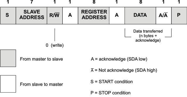 Figure 10. I2C Register Access With START or STOP
Registers that can be read are implemented using an I2C read operation, which can use the I2C combined format that changes data direction during the transaction. This transaction uses an I2C repeated START during the direction change.
8.5.7.2 I2C Combined Format
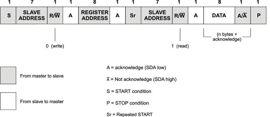 Figure 11. I2C Register Access With Repeated START
The UCD9081 also supports a feature that auto-increments the register address pointer for increased efficiency when accessing sequential blocks of data. It is not necessary to issue separate I2C transactions.
8.6 Register Maps
The UCD9081 allows all monitoring of the system through the I2C interface on the device. The following is the memory map of the supported registers in the system. The detail of each of these registers is given in the next section as well.
The UCD9081 supports functionality to increment the I2C register address value automatically when a register is being accessed to more efficiently access blocks of like registers. Table 1 also shows the amount that the register address is incremented for each register access.
Table 1. Register Access Adjustment
| REGISTER NAME | ADDRESS | ACCESS | ADJUSTMENT AFTER ACCESS |
|---|---|---|---|
| RAIL1H | 0x00 | r | +1 (0x01) |
| RAIL1L | 0x01 | r | +1 (0x02) |
| RAIL2H | 0x02 | r | +1 (0x03) |
| RAIL2L | 0x03 | r | +1 (0x04) |
| RAIL3H | 0x04 | r | +1 (0x05) |
| RAIL3L | 0x05 | r | +1 (0x06) |
| RAIL4H | 0x06 | r | +1 (0x07) |
| RAIL4L | 0x07 | r | +1 (0x08) |
| RAIL5H | 0x08 | r | +1 (0x09) |
| RAIL5L | 0x09 | r | +1 (0x0A) |
| RAIL6H | 0x0A | r | +1 (0x0B) |
| RAIL6L | 0x0B | r | +1 (0x0C) |
| RAIL7H | 0x0C | r | +1 (0x0D) |
| RAIL7L | 0x0D | r | +1 (0x0E) |
| RAIL8H | 0x0E | r | +1 (0x0F) |
| RAIL8L | 0x0F | r | –15 (0x00) |
| ERROR1 | 0x20 | r | +1 (0x21) |
| ERROR2 | 0x21 | r | +1 (0x22) |
| ERROR3 | 0x22 | r | +1 (0x23) |
| ERROR4 | 0x23 | r | +1 (0x24) |
| ERROR5 | 0x24 | r | +1 (0x25) |
| ERROR6 | 0x25 | r | –5 (0x20) |
| STATUS | 0x26 | r | 0 (0x26) |
| VERSION | 0x27 | r | 0 (0x27) |
| RAILSTATUS1 | 0x28 | r | +1 (0x29) |
| RAILSTATUS2 | 0x29 | r | –1 (0x28) |
| FLASHLOCK | 0x2E | rw | 0 (0x2E) |
| RESTART | 0x2F | w | 0 (0x2F) |
| WADDR1 | 0x30 | rw | +1 (0x31) |
| WADDR2 | 0x31 | rw | –1 (0x30) |
| WDATA1 | 0x32 | rw | +1 (0x33) |
| WDATA2 | 0x33 | rw | –1 (0x32) |
8.6.1 Register Descriptions
The following are the detailed descriptions of each of the UCD9081 I2C registers.
The following register bit conventions are used. Each register is shown with a key indicating the accessibility of each bit, and the initial condition after device initialization.
8.6.2 RAIL
For each of eight voltage rails, the UCD9081 has two registers that contain the rolling average voltage for the associated rail as measured by the device. This average voltage is maintained in real-time by the UCD9081 and is calculated as the output of a 4-TAP FIR filter. There are two registers for each voltage rail. One holds the least-significant 8 bits of the voltage and the other the most-significant 2 bits of the voltage. This is shown in Table 2.
Table 2. RAIL Register
| REGISTER NAME | ADDRESS | REGISTER CONTENTS |
|---|---|---|
| RAIL1H | 0x00 | RAIL1 voltage, bits 9:8 |
| RAIL1L | 0x01 | RAIL1 voltage, bits 7:0 |
| RAIL2H | 0x02 | RAIL2 voltage, bits 9:8 |
| RAIL2L | 0x03 | RAIL2 voltage, bits 7:0 |
| RAIL3H | 0x04 | RAIL3 voltage, bits 9:8 |
| RAIL3L | 0x05 | RAIL3 voltage, bits 7:0 |
| RAIL4H | 0x06 | RAIL4 voltage, bits 9:8 |
| RAIL4L | 0x07 | RAIL4 voltage, bits 7:0 |
| RAIL5H | 0x08 | RAIL5 voltage, bits 9:8 |
| RAIL5L | 0x09 | RAIL5 voltage, bits 7:0 |
| RAIL6H | 0x0A | RAIL6 voltage, bits 9:8 |
| RAIL6L | 0x0B | RAIL6 voltage, bits 7:0 |
| RAIL7H | 0x0C | RAIL7 voltage, bits 9:8 |
| RAIL7L | 0x0D | RAIL7 voltage, bits 7:0 |
| RAIL8H | 0x0E | RAIL8 voltage, bits 9:8 |
| RAIL8L | 0x0F | RAIL8 voltage, bits 7:0 |
A rail voltage is read with a 16b access. The auto-increment feature of the UCD9081 allows multiple rail voltages to be read with a single access.
A rail voltage is provided as a 10-bit binary value in an unsigned format, as shown in Figure 12.
 Figure 12. RAILVn Binary
The following formulas can be used to calculate the actual measured rail voltage.
Use Equation 1 for the actual measured rail voltage without an external voltage divider.
Use Equation 2 for the actual measured rail voltage with an external voltage divider.
8.6.3 ERROR
Error conditions are logged by the UCD9081 and are accessible to the user through reading the ERROR register. This is a 6-byte register is shown in Figure 13.
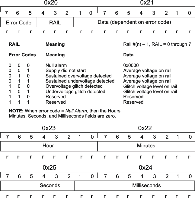 Figure 13. ERROR Register
Faults encountered during operation post error logs as described in Error Logging. This register set is used for reading the SRAM error log. They can also be used to read the FLASH error log when the UCD9081 is held in RESET. If the error log is empty, the ERROR register set returns all 0's (NULL ALARM) when read.
The values in registers 0x22 through 0x25 are reset to a value of 0 during UCD9081 RESET.
8.6.4 STATUS
STATUS is an 8-bit read-only register. This register provides real-time status information about the state of the UCD9081. Figure 14 shows the bit definitions.
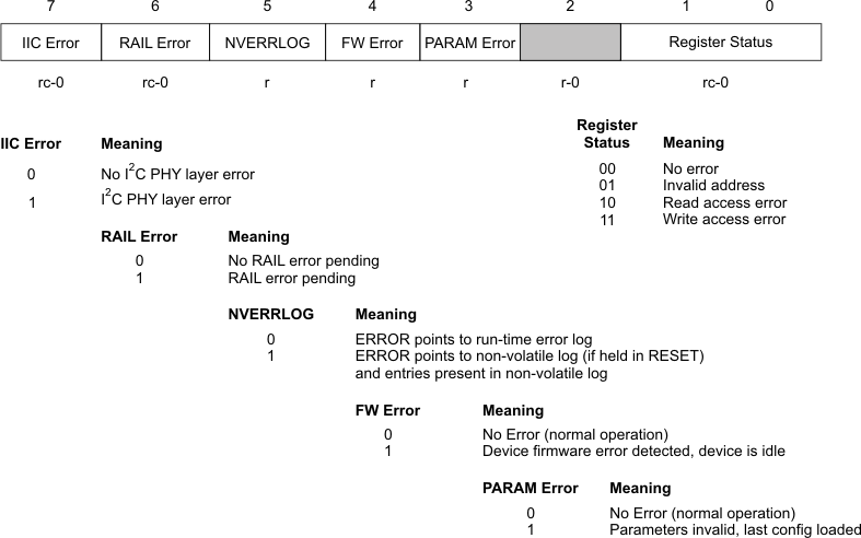 Figure 14. STATUS Register
Reading of the STATUS register clears the register except for the NVERRLOG bit, which is maintained until the device is reset. Descriptions of the different errors are below.
The IICERROR bit is set when an I2C access fails. This is most often a case where the user has accessed an invalid address or performed an illegal number of operations for a given register (for example, reading 3 bytes from a 2-byte register). In the event of an I2C error when the IICERROR is set, bits 1:0 of the STATUS register further define the nature of the error as shown in the preceding figure.
The RAIL error bit is set to alert the user to an issue with one of the voltage rails. When this bit is set, the user is advised to query the RAILSTATUS register to further ascertain which RAIL input(s) have an issue. The user may then query the ERROR registers to get further information about the nature of the error condition.
The NVERRLOG bit is set to 1 upon device RESET if the UCD9081 contains entries in the FLASH error log. This bit is the only bit that is not automatically cleared by a read of the STATUS register; this bit is only cleared during UCD9081 RESET (if the nonvolatile error log is empty).
The FW Error bit is set to 1 if the device firmware memory contents are corrupted.
The PARAM Error bit is set to 1 if the contents of the UCD9081 configuration memory are invalid. If this occurs, the UCD9081 loads the last known good configuration to ensure device reliability.
8.6.5 VERSION
The VERSION register provides the user with access to the device revision of the UCD9081. The format of this register is a nibble-based major/minor format as shown in Figure 15.
 Figure 15. VERSION Major/Minor Register
8.6.6 RAILSTATUS
The RAILSTATUS1 and RAILSTATUS2 registers are two 8-bit read-only registers that provide a bit mask to represent the error status of the rails as indicated in Figure 16.
 Figure 16. RAILSTATUS Registers
Bits 15:8 are RAILSTATUS1 and bits 7:0 are RAILSTATUS2. These are read as two 8-bit registers or as a single 16-bit register.
If a bit is set in these registers, then the ERROR register is read to further ascertain the specific error. Bits in the RAILSTATUS1 and RAILSTATUS2 registers are cleared when read.
8.6.7 FLASHLOCK
The FLASHLOCK register is used to lock and unlock the configuration memory on the UCD9081 when updating the configuration. Configuring the UCD9081 details this process.
Figure 17 shows the format for the FLASHLOCK register.
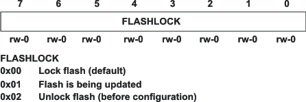 Figure 17. FLASHLOCK Register
8.6.8 RESTART
The RESTART register provides the capability for the I2C host to force a RESET or Shutdown of the UCD9081. This is an 8-bit register, and when a value of 0x00 is written to the register, the UCD9081 RESET occurs and the rails are re-sequenced. To respond to this I2C request properly, there is a 50-µs delay before the system is restarted, so that the I2C ACK can take place.
When a value of 0xC0 is written to the register, all rails and GPOs are shutdown according to the time delays specified in the system shutdown configuration. Once this procedure is complete, the UCD9081 continues monitoring.
8.6.9 WADDR and WDATA
To update the configuration on the UCD9081, four registers are provided. WADDR2 (address 15:8) and WADDR1 (address bits 7:0) specify the memory address. WDATA2 (data bits 15:8) and WDATA1 (data bits 7:0) specify the data written to or read from that memory address.
Figure 18 shows the format for the WADDR registers.
 Figure 18. WADDR Registers
To set the memory address that is accessed, write the LSB of the address to the WADDR1 register and the MSB of the address to the WADDR2 register. For example, to write the address 0x1234 to the device, set WADDR1 = 0x34 and WADDR2 = 0x12. Because these addresses support the auto-increment feature, the user can perform a single 16-bit write to WADDR1 to write the entire address.
Figure 19 shows the format for the WDATA registers.
 Figure 19. WDATA Registers
To set the value of the data that is written to the UCD9081, write the LSB of the data to the WDATA1 register and the MSB of the data to the WDATA2 register. For example, to write the data 0xBEEF to the device, set WDATA1 = 0xEF and WDATA2 = 0xBE. Because these addresses support the auto-increment feature, the user can perform a single 16-bit write to WDATA1 to write the entire data. To read the value of the data at the specified address, read the LSB from WDATA1 and the MSB from WDATA2.
These registers are used for updating the UCD9081 configuration as explained in Configuring the UCD9081.
8.6.10 Reading the FLASH Error Log
There are two ways to read the FLASH error log in the UCD9081. While the device is in RESET and the NVERRLOG bit in the STATUS register is set to a 1 (FLASH error logs present), the user may use the ERROR registers to read the log. During run-time, the FLASH error log can be accessed by performing an I2C read transaction starting at address 0x1000 with a length of 48 bytes.

