SLVS813C June 2008 – November 2016 UCD9081
PRODUCTION DATA.
- 1 Features
- 2 Applications
- 3 Description
- 4 Revision History
- 5 Pin Configuration and Functions
- 6 Specifications
- 7 Parameter Measurement Information
-
8 Detailed Description
- 8.1 Overview
- 8.2 Functional Block Diagram
- 8.3 Feature Description
- 8.4 Device Functional Modes
- 8.5 Programming
- 8.6 Register Maps
- 9 Application and Implementation
- 10Power Supply Recommendations
- 11Layout
- 12Device and Documentation Support
- 13Mechanical, Packaging, and Orderable Information
9 Application and Implementation
NOTE
Information in the following applications sections is not part of the TI component specification, and TI does not warrant its accuracy or completeness. TI’s customers are responsible for determining suitability of components for their purposes. Customers should validate and test their design implementation to confirm system functionality.
9.1 Application Information
9.1.1 Considerations for MONX Input Series Resistance, RS
RS is the series impedance between the sampled voltage source (low impedance power supply output) and the UCD9081 MONx input pin. This resistance can affect UCD9081 sampling accuracy if it is too large. In most cases (when the power supply being monitored has a lower VOUT than the UCD9081 voltage reference being used) this resistance is low and can be ignored. In cases where a voltage divider is used to scale the monitored voltage below the voltage reference, the impedance of this network must be chosen so that it does not adversely affect the analog to digital converter (ADC) conversion accuracy. The equivalent series impedance (RS) of the divider network is just the parallel combination of the pullup and pulldown resistors.
The UCD9081 has an internal clock (DCO) whose frequency is set by ROSC on pin 32. The DCO frequency can be affected by several factors including supply voltage and temperature. This clock is used by the ADC to set up an ADC sample or gate time (TGATE) at each MONx pin. The voltage sampled must be allowed to settle sufficiently during TGATE. The settling time is affected by the UCD9081 internal capacitance and RS. To allow for sufficient settling time over DCO frequency, supply voltage, and temperature variation, choose RS < 6 kΩ.
9.1.2 Estimating UCD9081 Reporting Accuracy Over Variations in ADC Voltage Reference
The UCD9081 uses a 10-bit ADC. The ADC in the UCD9081 derives its reference voltage (VR+ ) from either the external (VCC pin) or internal (VREF+) reference voltage to scale the digitally reported voltage. The least significant bit (LSB) voltage value is VLSB = VR+/2n where n = 10 and VR+ is the reference voltage used (either external VCC = 3.3 V nominal, or internal VREF+ = 2.5 V nominal). For external VR+ = VCC = 3.3 V, VLSB = 3.3 / 1024 = 3.22 mV and for internal VR+ = VREF+ = 2.5 V, VLSB = 2.5 / 1024 = 2.44 mV.
The error in the reported voltage is a function of the ADC linearity error(s) as well as variations in the ADC reference voltage. The total unadjusted error (ETUE) for the ADC in the UCD9081 is ±5 LSB and the variation of the internal 2.5-V reference is ±6% maximum. VTUE is calculated as VLSB × ETUE for the particular reference voltage used. The reported voltage error is the sum of the reference voltage error and the ADC total unadjusted error. At lower monitored voltages, ETUE may dominate reported error while at higher monitored voltages VR+ dominates the reported error. Reported error (percent) can be calculated using Equation 3.
where
- REFTOL is VR+ tolerance
- VACT is actual voltage monitored (at the UCD9081 MONx pin)
- VR+ is the nominal voltage of the ADC reference
Listed below are four examples using Equation 3 to estimate reported error:
- VR+ = 2.5 V, REFTOL = 6%, VACT = 0.25 V, RPTERR = 11.2%
- VR+ = 2.5 V, REFTOL = 6%, VACT = 2.25 V, RPTERR = 6.6%
- VR+ = 3.3 V, REFTOL = 1%, VACT = 0.25 V, RPTERR = 7.5%
- VR+ = 3.3 V, REFTOL = 1%, VACT = 2.25 V, RPTERR = 1.7%
In addition to the reporting errors due to ADC and voltage reference, there can be additional errors due to divider resistor tolerance when monitoring voltages higher than VR+. These errors can be added to the reporting error described above.
9.2 Typical Application
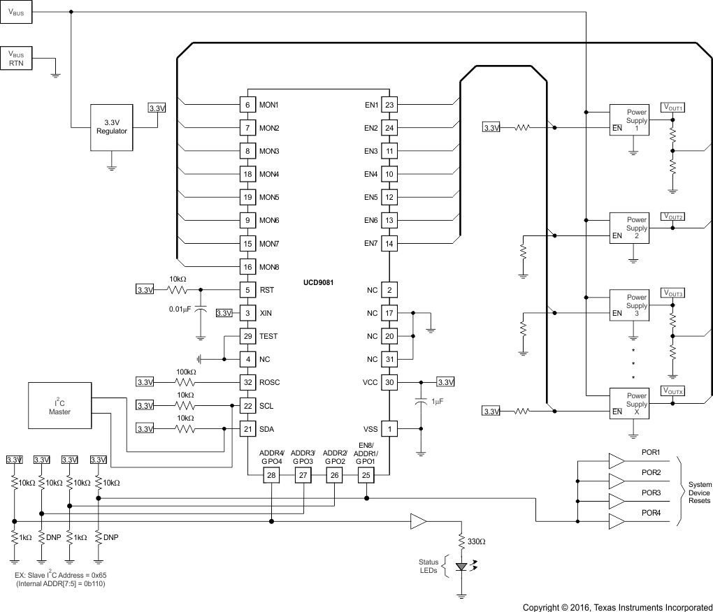
Figure 20 illustrates a typical power supply sequencing configuration. Power Supply 1 and Power Supply X require active low enables while Power Supply 2 and Power Supply 3 require active high enables. VOUT1 and VOUT3 exceed the selected A/D reference voltage so their outputs are divided before being sampled by the MON1 and MON3 inputs. VOUT2 and VOUTX are within the selected A/D reference voltage so their outputs can be sampled directly by the MON2 and MON7 inputs. Figure 20 illustrates the use of the GPO digital output pins to provide status and power on reset to other system devices.
 Figure 20. Typical Power Supply Sequencing Application
9.2.1 Design Requirements
RST pin must have a 10-kΩ pullup resistor to 3.3 V and 10-nF decoupling capacitor to ground. The component must be placed as close to the RST pin as possible.
9.2.2 Detailed Design Procedure
UCD9081 GUI can be used to design the device configuration. An USB-to-I2C Adapter from Texas Instruments can be used to connect GUI to I2C.
General design steps include:
- General rail setup
- Rail sequencing conditions setup
- Alarm action (fault response) setup
- System conditions setup
- General GPO setup
- GPO sequence setup
After configuration changes, click Store to Buffer to save the current entries to a GUI. Click Update Parameters and Sequence to permanently store the new configuration into the device data flash.
9.2.3 Application Curve
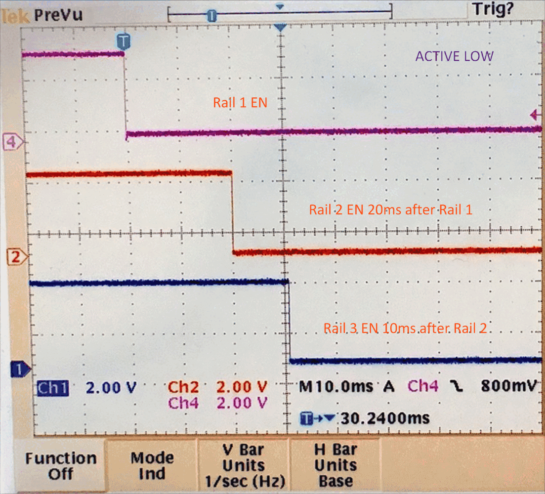
 Figure 21. Example Power-On Sequence