ZHCS952C June 2012 – January 2015 UCD8220-Q1
PRODUCTION DATA.
- 1 特性
- 2 应用
- 3 说明
- 4 修订历史记录
- 5 Pin Configuration and Functions
- 6 Specifications
- 7 Detailed Description
- 8 Application and Implementation
- 9 Power Supply Recommendations
- 10Layout
- 11器件和文档支持
- 12机械、封装和可订购信息
8 Application and Implementation
NOTE
Information in the following applications sections is not part of the TI component specification, and TI does not warrant its accuracy or completeness. TI’s customers are responsible for determining suitability of components for their purposes. Customers should validate and test their design implementation to confirm system functionality.
8.1 Application Information
The UCD8220-Q1 device can be configured for either peak current mode or voltage mode control. The device can be used to implement a variety of applications such as push-pull, half-bridge, or full-bridge converter.
8.2 Typical Application
Using the UCD8220-Q1 device in an application, a high degree of digital control can be achieved because the device integrates the PWM, logic, error amplifier, current limit, and drivers. In addition, the on-chip regulator provides power to the microcontroller. An example application is using the device in half-bridge power topology.
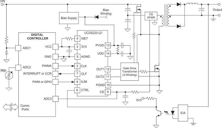 Figure 30. UCD8220-Q1 Typical Simplified Half-Bridge Converter Application Schematic
8.2.1 Design Requirements
When designing a half-bridge system, the key requirement is determining which functions should remain in the digital domain rather than the analog domain. The design shown in Figure 30 allows for a high degree of control over various blocks such as PWM, logic, error amplifier, current limit, and drivers. The UCD8220-Q1 closes the control loop for the power supply and provides the loop compensation. During operation, the UCD8220-Q1 monitors current and terminates the switching cycle safely if the value exceeds the current limit. By performing this task in the UCD8220-Q1, the device assists in real-time and full-time safety. The UCD8220-Q1 device provides notification of overcurrent events to the microcontroller. The notification of overcurrent events to the microcontroller allows the microcontroller to have a more complex response strategy. The firmware can, for example, direct the system to tolerate a finite number of current events, go to soft-stop, or shut down.
8.2.2 Detailed Design Procedure
Current limit is set through a simple resistor divider at the ISET pin. In the case of an overcurrent limit, the UCD8220-Q1 device sets the current flag (CF) pin high and the device is turned off by the host controller if the current limit exceeds a certain number of cycles. Depending upon the control method, the ISET resistor can be selected as previously mentioned.
8.2.2.1 Selecting the ISET Resistor for Voltage Mode Control
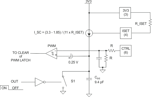 Figure 31. UCD8220-Q1 Configured in Voltage Mode Control With an Internal Timing Capacitor
When the ISET resistor is configured as shown in Figure 31 with the ISET resistor connected between the ISET pin and the 3V3 pin, the device is set up for voltage mode control. For purposes of voltage loop compensation the, voltage ramp is 1.4 V from the valley to the peak. Use Equation 5 to calculate the proper resistance for a desired clock frequency.

where
- fclk = desired clock frequency in Hz
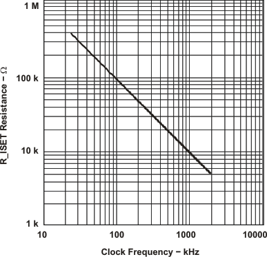 Figure 32. ISET Resistance Versus Clock Frequency
Figure 32 shows the nominal value of resistance to use for a desired clock frequency. For example, a clock frequency of 1000 kHz will require 10 kΩ of the ISET resistor. The UCD8220-Q1 device has two outputs controlled by push-pull logic and therefore the output ripple frequency is equal to the clock frequency and each output switches at half the clock frequency.
8.2.2.2 Selecting the ISET Resistor for Voltage Mode Control with Voltage Feed Forward
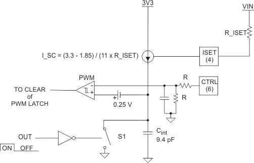 Figure 33. UCD8220-Q1 Configured in Voltage Mode Control with Voltage Feed Forward
When the ISET resistor is configured as shown in Figure 33 with the ISET resistor connected between the ISET pin and the input voltage, VIN, the device is configured for voltage mode control with voltage feed forward. For the purposes of voltage loop compensation, the voltage ramp is 1.4 V × VIN / VIN_max from the valley to the peak. Use Equation 6 to calculate the proper resistance for a desired clock frequency and input voltage range.

where
- fclk = Desired Clock Frequency in Hz
For a general discussion of the benefits of voltage mode control with voltage feed forward, see (5) in the 相关文档 section.
8.2.2.3 Selecting the ISET Resistor for Peak Current Mode Control with Internal Slope Compensation
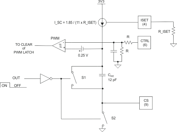 Figure 34. UCD8220-Q1 Configured in Peak Current Control with Internal Slope Compensation
When the ISET resistor is configured as shown in Figure 34 with the ISET resistor connected between the ISET pin and the AGND pin, the device is configured for peak current-mode control with internal slope compensation. The voltage at the ISET pin is 1.85 V so the internal slope compensation current, I_SC, being fed into the internal slope compensation capacitor is equal to 1.85 / (11 × R_ISET). Use Equation 7 to calculate the voltage slope at the PWM comparator input which is generated by this current.

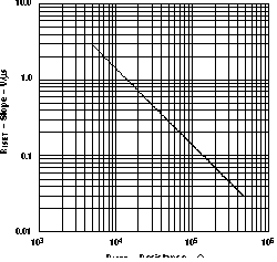 Figure 35. Slope vs R_ISET Resistance
The amount of slope compensation required depends on the design of the power stage and the output specifications. A general rule is to add an up-slope equal to the down slope of the output inductor. Refer to (1) and (8) in the 相关文档 section for a more detailed discussion regarding slope compensation in peak current mode controlled power stages.
8.2.3 Application Curves
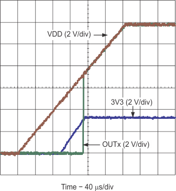
| CLK = CTRL = 3V3 |
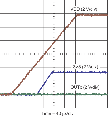
| CLK = AGND | CTRL = 3V3 |
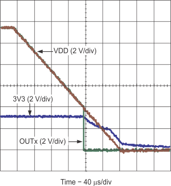
| CLK = CTRL = 3V3 |
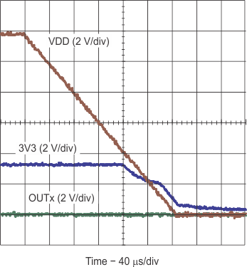
| CLK = AGND | CTRL = 3V3 |