ZHCS952C June 2012 – January 2015 UCD8220-Q1
PRODUCTION DATA.
- 1 特性
- 2 应用
- 3 说明
- 4 修订历史记录
- 5 Pin Configuration and Functions
- 6 Specifications
- 7 Detailed Description
- 8 Application and Implementation
- 9 Power Supply Recommendations
- 10Layout
- 11器件和文档支持
- 12机械、封装和可订购信息
7 Detailed Description
7.1 Overview
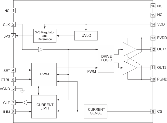
The UCD8220-Q1 device is a digitally managed analog PWM controller that is configured with push-pull drive logic.
In systems using the UCD8220-Q1 device, the PWM feedback loop is closed using the traditional analog methods. However, the UCD8220-Q1 includes circuitry to interpret a time-domain digital pulse train from a digital controller. The pulse train contains the operating frequency and maximum duty-cycle limit and therefore controls the power supply operation. The device circuitry eases the implementation of a converter with high-level control features without the added complexity or digital PWM-resolution limitations encountered when closing the voltage control-loop in the discrete time domain.
The UCD8220-Q1 device can be configured for either peak current-mode or voltage-mode control. The device provides a programmable current-limit function and a digital output current limit flag which can be monitored by the host controller. For fast switching speeds, the output stages use the TrueDrive output-circuit architecture, which delivers rated current of ±4-A into the gate of a MOSFET during the Miller plateau region of the switching transition. Finally the device also includes a 3.3-V, 10-mA linear regulator to provide power for the digital controller.
The UCD8220-Q1 device includes circuitry and features to ease implementing a converter that is managed by a microcontroller or a digital signal processor. Digitally managed power supplies provide software programmability and monitoring capability of the operation of the power supply, including:
- Switching frequency
- Synchronization
- DMAX
- V × S clamp
- Input UVLO start and stop voltage
- Input OVP start and stop voltage
- Soft-start profile
- Current-limit operation
- Shutdown
- Temperature shutdown
7.2 Functional Block Diagram

7.3 Feature Description
7.3.1 CLK Input Time-Domain Digital Pulse Train
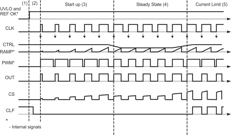
While the loop is closed in the analog domain, the UCD8220-Q1 device is managed by a time-domain digital pulse train from a digital controller. The pulse train, shown as CLK in Figure 27, contains the operating frequency and maximum duty-cycle limit and therefore controls the power supply operation as previously listed. The pulse train uses a Texas Instruments communication protocol which is a proprietary communication system that provides control of the power supply operation through software programming. The rising edge of the CLK signal represents the switching frequency. Figure 27 depicts the operation of the UCD8220-Q1 device in one of five modes. At the time when the internal signal REF OK is low, the UCD8220-Q1 device is not ready to accept CLK inputs. When the REF OK signal goes high, then the device is ready to process inputs. While the CLK input is low, the outputs are disabled and the CLK signal is used as an enable input. When the digital controller completes the initialization routine and verifies that all voltages are within operating range, then the controller begins the soft-start procedure by slowly ramping up the duty cycle of the CLK signal, while maintaining the desired switching frequency. The CLK duty cycle continues to increase until it reaches steady-state where the analog control loop takes over and regulates the output voltage to the desired set point. During steady state, the duty cycle of the CLK pulse can be set using a volt-second product calculation to protect the primary of the power transformer from saturation during transients.
When the power supply detects an overcurrent event, it enters the current-limit mode where the outputs are quickly turned off and the CLF signal is set high to notify the digital controller that the last power pulse was truncated. This technique is beneficial because it allows the digital controller to decide how to handle this overcurrent event while providing some protection to the other components being supplied by this device.
The software is now in charge of the response to overcurrent events. In typical analog designs, the power supply response to overcurrent is hardwired in the silicon. With this method, the user can configure the response differently for different applications. For example, the software can be configured to latch-off the power supply in response the first overcurrent event, or to allow a fixed number of current-limit events, so that the supply is capable of starting up into a capacitive load. The user can also configure the supply to enter into hiccup mode immediately or after a certain number of current-limit events. As described later in this data sheet, the current limit threshold can be varied in time to create unique current limit profiles. For example, the current limit set point can be set high for a predefined number of cycles to blow a manual fuse, and can be reduced down to protect the system in the event of a faulty fuse.
 Figure 27. Timing and Circuit Operation Diagram
7.3.2 Current Sensing and Protection
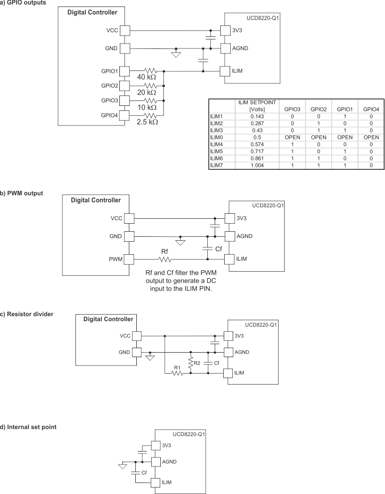
 Figure 28. ILIM Settings
7.3.3 Handshaking
The UCD8220-Q1 device has a built-in handshaking feature to facilitate efficient start-up of the digitally managed power supply. At start-up the CLF flag is held high until all the internal and external supply voltages of the UCD8220-Q1 device is within its operating range. When the supply voltages are within acceptable limits, the CLF flag goes low and the device processes the CLK signals. The digital controller should monitor the CFL flag at start-up and wait for the CLF flag to go low before sending CLK pulses to the UCD8220-Q1 device.
7.3.4 Driver Output
The high-current output stage of the UCD8220-Q1 device is capable of supplying ±4-A peak current pulses and swings to both the PVDD and PGND pins.
The drive output uses the TI's TrueDrive output-circuit architecture, which delivers rated current into the gate of a MOSFET when it is most needed, during the Miller plateau region of the switching transition providing efficiency gains.
The TrueDrive integrated circuit consists of pullup and pulldown circuits with bipolar and MOSFET transistors in parallel. The peak output current rating is the combined current from the bipolar and MOSFET transistors. This hybrid output stage also allows efficient current sourcing at low supply voltages.
7.3.5 Source and Sink Capabilities During Miller Plateau
Large power MOSFETs present a large load to the control circuitry. Proper drive is required for efficient, reliable operation. The UCD8220-Q1 driver has been optimized to provide maximum drive to a power MOSFET during the Miller plateau region of the switching transition. This interval occurs while the drain voltage is swinging between the voltage levels dictated by the power topology, requiring the charging or discharging of the drain-gate capacitance with current supplied or removed by the driver device. See (5) in the 相关文档 section.
7.3.6 Drive Current and Power Requirements
The UCD8220-Q1 device contains drivers that can deliver high current into a MOSFET gate for a period of several hundred nanoseconds. High-peak current is required to turn on a MOSFET. To turn off a MOSFET, the driver is required to sink a similar amount of current to ground. This cycle repeats at the operating frequency of the power device.
For additional information on the current required to drive a power MOSFET and other capacitive-input switching devices, see (5) in the 相关文档 section.
When a driver device is tested with a discrete, capacitive load, calculating the power that is required from the bias supply is fairly simple. Use Equation 1 to calculate the energy that must be transferred from the bias supply to charge the capacitor.

where
- C is the load capacitor
- V is the bias voltage feeding the driver
An equal amount of energy is transferred to ground when the capacitor is discharged. This transfer of energy results in a power loss which is calculated with Equation 2.

where
- f is the switching frequency
This power is dissipated in the resistive elements of the circuit. Thus, with no external resistor between the driver and gate, this power is dissipated inside the driver. Half of the total power is dissipated when the capacitor is charged, and the other half is dissipated when the capacitor is discharged.
Use Equation 3 to calculate the power loss with the following values: VDD = 12 V, CLOAD = 2.2 nF, and f = 300 kHz.

Use Equation 4 to calculate the current with a 12-V supply.

7.3.7 Clearing the Current-Limit Flag (CLF)
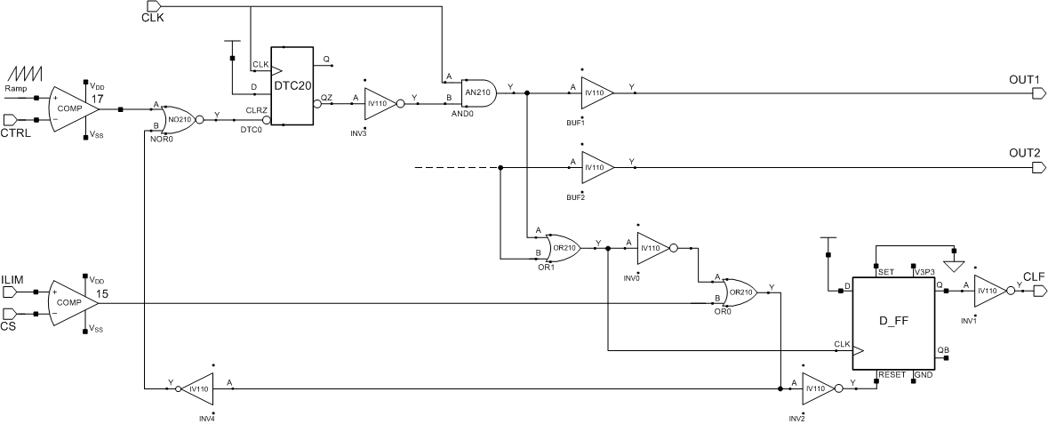
In the UCD8220-Q1 design, the CLF signal is cleared by the comparator (compares the voltage between the CS and ILIM pins) output. However, the comparator output is enabled by the OUTx pin. Therefore, the CLF signal does not clear (go low) unless one or both OUTx pins are on, which enables the comparator output. Pulling the CTRL pin high turns the OUTx pin on which is why the CLF flag only clears when CTRL is high (greater than 0.45 to 0.6 V). Therefore, anything that turns on the OUTs pins enables the comparator, and if V_CS is less than V_ILIM, the comparator output clears the CLF signal. The CLF signal goes low during the next rising edge on the CLK pin after these conditions are met.
 Figure 29. Logic Circuit for CLF
7.4 Device Functional Modes
The device has no additional functional modes.