ZHCS952C June 2012 – January 2015 UCD8220-Q1
PRODUCTION DATA.
- 1 特性
- 2 应用
- 3 说明
- 4 修订历史记录
- 5 Pin Configuration and Functions
- 6 Specifications
- 7 Detailed Description
- 8 Application and Implementation
- 9 Power Supply Recommendations
- 10Layout
- 11器件和文档支持
- 12机械、封装和可订购信息
10 Layout
10.1 Layout Guidelines
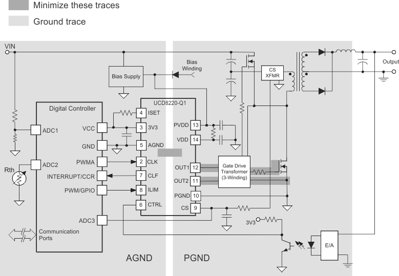
In a MOSFET driver operating at high frequency, minimizing stray inductance to minimize overshoot, undershoot, and ringing is critical. The low output impedance of the drivers produces waveforms with high di/dt which tends to induce ringing in the parasitic inductances. Connecting the driver device close to the MOSFETs is advantageous. To reduce ringing, minimize the trace inductance from OUT 1 and OUT 2 to the MOSFET input. Connecting the PGND and AGND pins to the PowerPAD integrated circuit package with a thin trace is recommended. Ensuring that the voltage potential between these two pins does not exceed 0.3 V is critical. The use of schottky diodes on the outputs to the PGND and PVDD pins is recommended when driving gate transformers. See (3) in the 相关文档 section for a description of proper pad layout for the PowerPAD integrated circuit package.
10.2 Layout Example
 Figure 40. UCD8220-Q1 Layout Example
10.3 Thermal Considerations
The useful range of a driver is greatly affected by the drive power requirements of the load and the thermal characteristics of the device package. In order for a power driver to be useful over a particular temperature range the package must allow for the efficient removal of the heat produced while keeping the junction temperature within rated limits. The UCD8220-Q1 device is available in the PowerPAD integrated circuit package, HTSSOP, to cover a range of application requirements. The package has an exposed pad to enhance thermal conductivity from the semiconductor junction.
As shown in (4) in the 相关文档 section, the PowerPAD integrated circuit packages offer a leadframe die pad that is exposed at the base of the package. This pad is soldered to the copper on the PC board (PCB) directly underneath the device package, reducing the RθJA down to 37.47°C/W. The PC board must be designed with thermal lands and thermal vias to complete the heat removal subsystem, as discussed in (3) in the 相关文档 section.
Note that the PowerPAD integrated circuit package is not directly connected to any leads of the package. However, the PowerPAD is electrically and thermally connected to the substrate which is the ground of the device. The PowerPAD integrated circuit package should be connected to the quiet ground of the circuit.