ZHCSD93A january 2015 – december 2020 UCC28700-Q1
PRODUCTION DATA
- 1
- 1 特性
- 2 应用
- 3 说明
- 4 Revision History
- 5 Pin Configuration and Functions
- 6 Specifications
- 7 Detailed Description
-
8 Applications and Implementation
- 8.1 Application Information
- 8.2
Typical Application
- 8.2.1 Design Requirements
- 8.2.2
Detailed Design Procedure
- 8.2.2.1 Transformer Parameter Verification
- 8.2.2.2 Output Capacitance
- 8.2.2.3 VDD Capacitance, CDD
- 8.2.2.4 VDD Start-Up Resistance, RSTR
- 8.2.2.5 VS Resistor Divider, Line Compensation, and Cable Compensation
- 8.2.2.6 Input Bulk Capacitance and Minimum Bulk Voltage
- 8.2.2.7 Transformer Turns Ratio, Inductance, Primary-Peak Current
- 8.2.2.8 Standby Power Estimate
- 8.2.3 Application Curves
- 9 Power Supply Recommendations
- 10Layout
-
11Device and Documentation Support
- 11.1
Device Support
- 11.1.1
Device Nomenclature
- 11.1.1.1 Capacitance Terms in Farads
- 11.1.1.2 Duty Cycle Terms
- 11.1.1.3 Frequency Terms in Hertz
- 11.1.1.4 Current Terms in Amperes
- 11.1.1.5 Current and Voltage Scaling Terms
- 11.1.1.6 Transformer Terms
- 11.1.1.7 Power Terms in Watts
- 11.1.1.8 Resistance Terms in Ω
- 11.1.1.9 Timing Terms in Seconds
- 11.1.1.10 Voltage Terms in Volts
- 11.1.1.11 AC Voltage Terms in VRMS
- 11.1.1.12 Efficiency Terms
- 11.1.1
Device Nomenclature
- 11.2 Documentation Support
- 11.3 Trademarks
- 11.1
Device Support
- Mechanical, Packaging, and Orderable Information
8.2.2.5 VS Resistor Divider, Line Compensation, and Cable Compensation
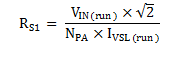
The VS divider resistors determine the output voltage regulation point of the flyback converter, also the high-side divider resistor (RS1) determines the line voltage at which the controller enables continuous DRV operation. RS1 is initially determined based on transformer auxiliary to primary turns ratio and desired input voltage operating threshold.
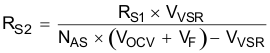
The low-side VS pin resistor is selected based on desired VO regulation voltage.
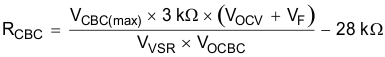
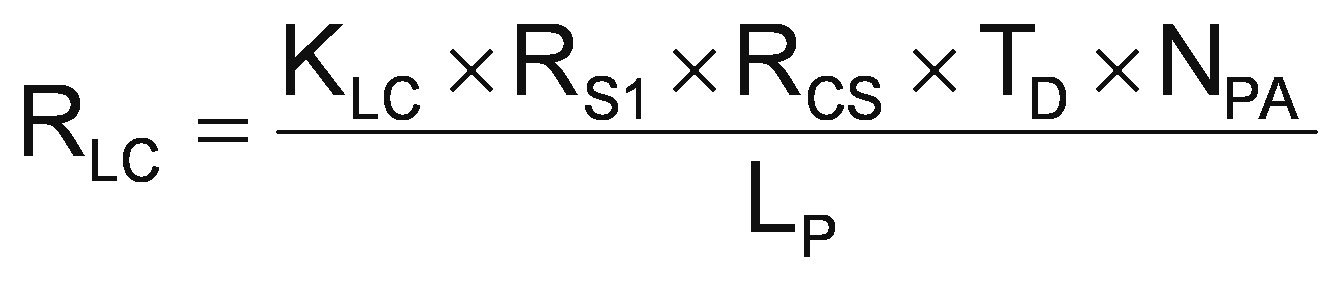
The UCC28700-Q1 can maintain tight constant-current regulation over input line by utilizing the line compensation feature. The line compensation resistor (RLC) value is determined by current flowing in RS1 and expected gate drive and MOSFET turn-off delay. Assume a 50-ns internal delay in the UCC28700-Q1.
On the UCC28700-Q1 which has adjustable cable compensation, the resistance for the desired compensation level at the output terminals can be determined using the equation below.