ZHCSD93A january 2015 – december 2020 UCC28700-Q1
PRODUCTION DATA
- 1
- 1 特性
- 2 应用
- 3 说明
- 4 Revision History
- 5 Pin Configuration and Functions
- 6 Specifications
- 7 Detailed Description
-
8 Applications and Implementation
- 8.1 Application Information
- 8.2
Typical Application
- 8.2.1 Design Requirements
- 8.2.2
Detailed Design Procedure
- 8.2.2.1 Transformer Parameter Verification
- 8.2.2.2 Output Capacitance
- 8.2.2.3 VDD Capacitance, CDD
- 8.2.2.4 VDD Start-Up Resistance, RSTR
- 8.2.2.5 VS Resistor Divider, Line Compensation, and Cable Compensation
- 8.2.2.6 Input Bulk Capacitance and Minimum Bulk Voltage
- 8.2.2.7 Transformer Turns Ratio, Inductance, Primary-Peak Current
- 8.2.2.8 Standby Power Estimate
- 8.2.3 Application Curves
- 9 Power Supply Recommendations
- 10Layout
-
11Device and Documentation Support
- 11.1
Device Support
- 11.1.1
Device Nomenclature
- 11.1.1.1 Capacitance Terms in Farads
- 11.1.1.2 Duty Cycle Terms
- 11.1.1.3 Frequency Terms in Hertz
- 11.1.1.4 Current Terms in Amperes
- 11.1.1.5 Current and Voltage Scaling Terms
- 11.1.1.6 Transformer Terms
- 11.1.1.7 Power Terms in Watts
- 11.1.1.8 Resistance Terms in Ω
- 11.1.1.9 Timing Terms in Seconds
- 11.1.1.10 Voltage Terms in Volts
- 11.1.1.11 AC Voltage Terms in VRMS
- 11.1.1.12 Efficiency Terms
- 11.1.1
Device Nomenclature
- 11.2 Documentation Support
- 11.3 Trademarks
- 11.1
Device Support
- Mechanical, Packaging, and Orderable Information
7.3.1.3 VS (Voltage-Sense)
The VS pin is connected to a resistor divider from the auxiliary winding to ground. The output-voltage feedback information is sampled at the end of the transformer secondary current demagnetization time to provide an accurate representation of the output voltage. Timing information to achieve valley-switching and to control the duty cycle of the secondary transformer current is determined by the waveform on the VS pin. Avoid placing a filter capacitor on this input which would interfere with accurate sensing of this waveform.
The VS pin also senses the bulk capacitor voltage to provide for AC-input run and stop thresholds, and to compensate the current-sense threshold across the AC-input range. This information is sensed during the MOSFET on-time. For the AC-input run/stop function, the run threshold on VS is 220 µA and the stop threshold is 80 µA. The values for the auxiliary voltage divider upper-resistor RS1 and lower-resistor RS2 can be determined by the equations below.
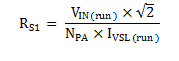
where
- NPA is the transformer primary-to-auxiliary turns ratio,
- VIN(run) is the AC RMS voltage to enable turn-on of the controller (run),
- IVSL(run) is the run-threshold for the current pulled out of the VS pin during the MOSFET on-time. (see the Section 6.5 table)
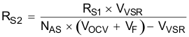
where
- VOCV is the converter regulated output voltage,
- VF is the output rectifier forward drop at near-zero current,
- NAS is the transformer auxiliary to secondary turns ratio,
- RS1 is the VS divider high-side resistance,
- VVSR is the CV regulating level at the VS input (see the Section 6.5 table).