ZHCSGE8A June 2017 – August 2018 UCC27712
PRODUCTION DATA.
- 1 特性
- 2 应用
- 3 说明
- 4 修订历史记录
- 5 Pin Configuration and Functions
- 6 Specifications
- 7 Detailed Description
-
8 Application and Implementation
- 8.1 Application Information
- 8.2
Typical Application
- 8.2.1 Design Requirements
- 8.2.2
Detailed Design Procedure
- 8.2.2.1 Selecting HI and LI Low Pass Filter Components (RHI, RLI, CHI, CLI)
- 8.2.2.2 Selecting Bootstrap Capacitor (CBOOT)
- 8.2.2.3 Selecting VDD Bypass/Holdup Capacitor (CVDD) and Rbias
- 8.2.2.4 Selecting Bootstrap Resistor (RBOOT)
- 8.2.2.5 Selecting Gate Resistor RON/ROFF
- 8.2.2.6 Selecting Bootstrap Diode
- 8.2.2.7 Estimate the UCC27712 Power Losses (PUCC27712)
- 8.2.2.8 Estimating Junction Temperature
- 8.2.2.9 Operation With IGBT's
- 8.2.3 Application Curves
- 9 Power Supply Recommendations
- 10Layout
- 11器件和文档支持
- 12机械、封装和可订购信息
6.6 Dynamic Electrical Characteristics
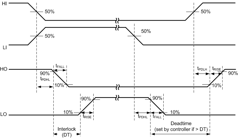
At VDD = VHB = 15 V, COM = VHS = 0, all voltages are with respect to COM, no load on LO and HO, –40°C < TJ < +125°C (unless otherwise noted). Currents are positive into and negative out of the specified terminal.| PARAMETER | TEST CONDITIONS | MIN | NOM | MAX | UNIT | |
|---|---|---|---|---|---|---|
| DYNAMIC CHARACTERISTICS | ||||||
| tPDLH | Turn-on propagation delay (without deadtime) | LI to LO, HI to HO, HS = COM = 0 V | 100 | 160 | ns | |
| tPDHL | Turn-off propagation delay | LI to LO, HI to HO, HS = COM = 0 V | 100 | 160 | ||
| tPDRM | Low-to-high delay matching | 5 | 30 | |||
| tPDFM | High-to-low delay matching | 12 | 30 | |||
| tRISE | Turn-on rise time | 10% to 90%, HO/LO with 1000-pF load | 16 | 50 | ||
| tFALL | Turn-off fall time | 10% to 90%, HO/LO with 1000-pF load | 10 | 30 | ||
| tON | Minimum HI/LI ON pulse that changes output state | 0-V to 5-V input signal on HI and LI pins | 25 | 45 | ||
| tOFF | Minimum HI/LI OFF pulse that changes output state | 5-V to 0-V input signal on HI and LI pins | 35 | 45 | ||
| DT | Deadtime | Internal deadtime for Interlock | 100 | 150 | 200 | |
 Figure 1. Typical Test Timing Diagram