ZHCSG75E April   2017  – April 2018 TUSB544

PRODUCTION DATA.  

  1. 特性
  2. 应用
  3. 说明
    1.     Device Images
      1.      简化原理图
  4. 修订历史记录
  5. Pin Configuration and Functions
    1.     Pin Functions
  6. Specifications
    1. 6.1  Absolute Maximum Ratings
    2. 6.2  ESD Ratings
    3. 6.3  Recommended Operating Conditions
    4. 6.4  Thermal Information
    5. 6.5  Power Supply Characteristics
    6. 6.6  DC Electrical Characteristics
    7. 6.7  AC Electrical Characteristics
    8. 6.8  Timing Requirements
    9. 6.9  Switching Characteristics
    10. 6.10 Typical Characteristics
  7. Detailed Description
    1. 7.1 Overview
    2. 7.2 Functional Block Diagram
    3. 7.3 Feature Description
      1. 7.3.1 USB 3.1
      2. 7.3.2 DisplayPort
      3. 7.3.3 4-Level Inputs
      4. 7.3.4 Receiver Linear Equalization
    4. 7.4 Device Functional Modes
      1. 7.4.1 Device Configuration in GPIO Mode
      2. 7.4.2 Device Configuration in I2C Mode
      3. 7.4.3 DisplayPort Mode
      4. 7.4.4 Custom Alternate Mode
      5. 7.4.5 Linear EQ Configuration
      6. 7.4.6 Adjustable VOD Linear Range and DC Gain
      7. 7.4.7 USB3.1 modes
      8. 7.4.8 Operation Timing – Power Up
    5. 7.5 Programming
      1. 7.5.1 The Following Procedure Should be Followed to Write to TUSB544 I2C Registers:
      2. 7.5.2 The Following Procedure Should be Followed to Read the TUSB544 I2C Registers:
      3. 7.5.3 The Following Procedure Should be Followed for Setting a Starting Sub-Address for I2C Reads:
    6. 7.6 Register Maps
      1. 7.6.1 TUSB544 Registers
        1. 7.6.1.1  GENERAL_4 Register (Offset = Ah) [reset = 1h]
          1. Table 13. GENERAL_4 Register Field Descriptions
        2. 7.6.1.2  GENERAL_5 Register (Offset = Bh) [reset = 0h]
          1. Table 14. GENERAL_5 Register Field Descriptions
        3. 7.6.1.3  GENERAL_6 Register (Offset = Ch) [reset = 0h]
          1. Table 15. GENERAL_6 Register Field Descriptions
        4. 7.6.1.4  DISPLAYPORT_1 Register (Offset = 10h) [reset = 0h]
          1. Table 16. DISPLAYPORT Register Field Descriptions
        5. 7.6.1.5  DISPLAYPORT_2 Register (Offset = 11h) [reset = 0h]
          1. Table 17. DISPLAYPORT_2 Register Field Descriptions
        6. 7.6.1.6  DISPLAYPORT_3 Register (Offset = 12h) [reset = 0h]
          1. Table 18. DISPLAYPORT_3 Register Field Descriptions
        7. 7.6.1.7  DISPLAYPORT_4 Register (Offset = 13h) [reset = 0h]
          1. Table 19. DISPLAYPORT_4 Register Field Descriptions
        8. 7.6.1.8  DISPLAYPORT_5 Register (Offset = 1Bh) [reset = 0h]
          1. Table 20. DISPLAYPORT_5 Register Field Descriptions
        9. 7.6.1.9  USB3.1_1 Register (Offset = 20h) [reset = 0h]
          1. Table 21. USB3.1 Register Field Descriptions
        10. 7.6.1.10 USB3.1_2 Register (Offset = 21h) [reset = 0h]
          1. Table 22. USB3.1_2 Register Field Descriptions
        11. 7.6.1.11 USB3.1_3 Register (Offset = 22h) [reset = 0h]
          1. Table 23. USB3.1_3 Register Field Descriptions
        12. 7.6.1.12 USB3.1_4 Register (Offset = 23h) [reset = 23h]
          1. Table 24. USB3.1_4 Register Field Descriptions
  8. Application and Implementation
    1. 8.1 Application Information
    2. 8.2 Typical Application
      1. 8.2.1 Design Requirements
      2. 8.2.2 Detailed Design Procedure
      3. 8.2.3 Application Curve
    3. 8.3 System Examples
      1. 8.3.1 USB 3.1 only (USB/DP Alternate Mode)
      2. 8.3.2 USB3.1 and 2 lanes of DisplayPort
      3. 8.3.3 DisplayPort Only
      4. 8.3.4 USB 3.1 only (USB/Custom Alternate Mode)
      5. 8.3.5 USB3.1 and 1 Lane of Custom Alt Mode
      6. 8.3.6 USB3.1 and 2 Lane of Custom Alt Mode
      7. 8.3.7 USB3.1 and 4 Lane of Custom Alt Mode
  9. Power Supply Recommendations
  10. 10Layout
    1. 10.1 Layout Guidelines
    2. 10.2 Layout Example
  11. 11器件和文档支持
    1. 11.1 文档支持
      1. 11.1.1 相关文档
    2. 11.2 接收文档更新通知
    3. 11.3 社区资源
    4. 11.4 商标
    5. 11.5 静电放电警告
    6. 11.6 术语表
  12. 12机械、封装和可订购信息

封装选项

机械数据 (封装 | 引脚)
散热焊盘机械数据 (封装 | 引脚)
订购信息

Detailed Design Procedure

A typical usage of the TUSB544 device is shown in Figure 35. The device can be controlled either through its GPIO pins or through its I2C interface. In the example shown below, a Type-C PD controller is used to configure the device through the I2C interface. In I2C mode, the equalization settings for each receiver can be independently controlled through I2C registers. For this reason, all of the equalization pins (UEQ[1:0] and DEQ[1:0]) can be left unconnected. If these pins are left unconnected, the TUSB544 7-bit I2C slave address will be 12h because both UEQ1/A1 and UEQ0/A0 will be at pin level "F". If a different I2C slave address is desired, UEQ1/A1 and UEQ0/A0 pins should be set to a level which produces the desired I2C slave address.
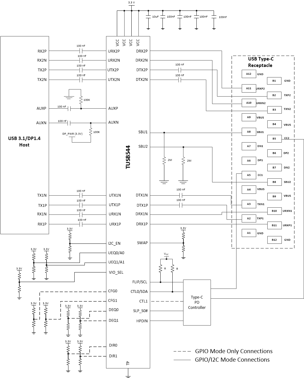
TUSB544 Typ_Application_Schematic.gifFigure 35. Typical Application Circuit