ZHCSEO6B DECEMBER   2012  – December 2015 TPS92560

PRODUCTION DATA.  

  1. 特性
  2. 应用
  3. 说明
  4. 修订历史记录
  5. Pin Configuration and Functions
  6. Specifications
    1. 6.1 Absolute Maximum Ratings
    2. 6.2 ESD Ratings
    3. 6.3 Recommended Operating Conditions
    4. 6.4 Thermal Information
    5. 6.5 Electrical Characteristics
    6. 6.6 Typical Characteristics
  7. Detailed Description
    1. 7.1 Overview
    2. 7.2 Functional Block Diagram
    3. 7.3 Feature Description
      1. 7.3.1 VCC Regulator
      2. 7.3.2 MOSFET Driver
      3. 7.3.3 ADJ Pin
        1. 7.3.3.1 Output OVP
      4. 7.3.4 AC1 and AC2 Pins
      5. 7.3.5 Detection of Power Source
      6. 7.3.6 Current Regulation
      7. 7.3.7 Switching Frequency (Boost Configuration)
      8. 7.3.8 Inductor Selection (Boost Configuration)
      9. 7.3.9 Input Surge Voltage Protection
    4. 7.4 Device Functional Modes
      1. 7.4.1 Thermal Shutdown
  8. Application and Implementation
    1. 8.1 Application Information
    2. 8.2 Typical Applications
      1. 8.2.1 Boost Application Design Example
        1. 8.2.1.1 Design Requirements
        2. 8.2.1.2 Detailed Design Procedure
          1. 8.2.1.2.1 Calculate Values for the ADJ Resistors
          2. 8.2.1.2.2 Calculate the Sense Voltage and Sense Resistor Value
          3. 8.2.1.2.3 Calculate the Inductor Value
        3. 8.2.1.3 Application Curve
      2. 8.2.2 Boost Application Circuit With LED Current Regulation
        1. 8.2.2.1 Design Requirements
        2. 8.2.2.2 Application Curves
      3. 8.2.3 SEPIC Application Circuit With LED Current Regulation
        1. 8.2.3.1 Design Requirements
        2. 8.2.3.2 Application Curves
  9. Power Supply Recommendations
  10. 10Layout
    1. 10.1 Layout Guidelines
    2. 10.2 Layout Example
  11. 11器件和文档支持
    1. 11.1 社区资源
    2. 11.2 商标
    3. 11.3 静电放电警告
    4. 11.4 Glossary
  12. 12机械、封装和可订购信息

封装选项

机械数据 (封装 | 引脚)
散热焊盘机械数据 (封装 | 引脚)
订购信息

10 Layout

10.1 Layout Guidelines

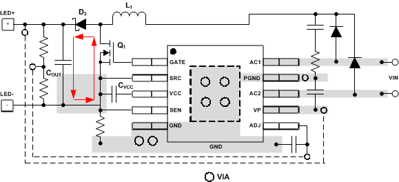
The VP input capacitor and ADJ resistors/capacitor should be placed as close to the IC as possible. The VCC capacitor should also be placed close to the device. Minimize the switching node area (connection between Q1, L1, and D3) and keep the discontinuous current switching path as short as possible. This includes the loop formed by Q1, COUT, and the diode D3 (designated by the red arrows). The ground connections for the TPS92560 and RSEN should be tide closely together with a solid ground plane. The node connecting the SEN pin, SRC pin, the source of Q1, CVCC, and COUT should be small with all components connected closely together.

10.2 Layout Example
TPS92560 snvs900_layout.gif Figure 26. TPS92560 Layout Example