ZHCS834G June 2011 – March 2020 TPS7A63-Q1 , TPS7A6401-Q1
PRODUCTION DATA.
- 1 特性
- 2 应用
- 3 说明
- 4 修订历史记录
- 5 Pin Configuration and Functions
- 6 Specifications
-
7 Detailed Description
- 7.1 Overview
- 7.2 Functional Block Diagrams
- 7.3 Feature Description
- 7.4 Device Functional Modes
- 8 Application and Implementation
- 9 Power Supply Recommendations
- 10Layout
- 11器件和文档支持
- 12机械、封装和可订购信息
封装选项
机械数据 (封装 | 引脚)
散热焊盘机械数据 (封装 | 引脚)
订购信息
10.1.1.1 Example
If IOUT = 100 mA, VOUT = 5 V, VIN = 14 V, IQUIESCENT = 250 µA, and RθJA= 50°C/W, the continuous power dissipated in the device is 0.9 W. The rise in junction temperature due to power dissipation is 45°C. For a maximum junction temperature of 150°C, the maximum ambient air temperature at which the device can operate is 105°C.
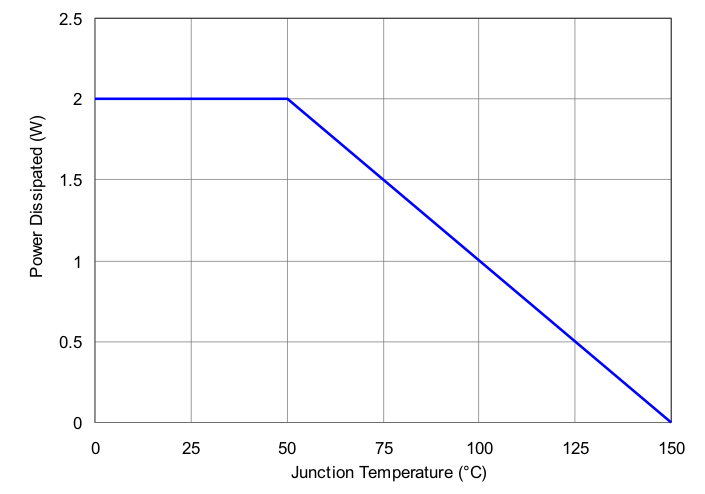
For adequate heat dissipation, TI recommends soldering the thermal pad (exposed heat sink) to the thermal land pad on the PCB. Doing this provides a heat conduction path from the die to the PCB and reduces overall package thermal resistance. Power derating curves for the TPS7A63-Q1 and TPS7A6401-Q1 PWP package and TPS7A6333-Q1 DRK are comparable; see Figure 35.
 Figure 35. Power Derating Curve
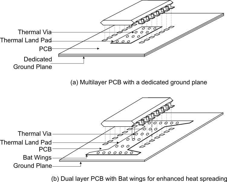
 For optimum thermal performance, TI recommends using a high-K PCB with thermal vias between the ground plane and solder pad or thermal land pad; see Figure 36 (a) and (b). Further, use a thicker ground plane and a thermal land pad with a larger surface area to inprove considerably the heat-spreading capabilities of a PCB. For a two-layer PCB, a bat wing layout can enhance the heat-spreading capabilities.
 Figure 36. Using Multilayer PCB and Thermal Vias for Adequate Heat Dissipation
 Keeping other factors constant, surface area of the thermal land pad contributes to heat dissipation only to a certain extent.