SLVSAY9F December 2012 – March 2016 TPS65320-Q1
PRODUCTION DATA.
- 1 Features
- 2 Applications
- 3 Description
- 4 Revision History
- 5 Pin Configuration and Functions
- 6 Specifications
-
7 Detailed Description
- 7.1 Overview
- 7.2 Functional Block Diagram
- 7.3
Feature Description
- 7.3.1
Buck Regulator
- 7.3.1.1 Fixed-Frequency PWM Control
- 7.3.1.2 Slope Compensation Output
- 7.3.1.3 Pulse-Skip Eco-mode™ Control Scheme
- 7.3.1.4 Dropout Operation and Bootstrap Voltage (BOOT)
- 7.3.1.5 Error Amplifier
- 7.3.1.6 Voltage Reference
- 7.3.1.7 Adjusting the Output Voltage
- 7.3.1.8 Soft-Start and Tracking Pin (SS/TR)
- 7.3.1.9 Overload Recovery Circuit
- 7.3.1.10 Constant Switching Frequency and Timing Resistor (RT/CLK Pin)
- 7.3.1.11 Overcurrent Protection and Frequency Shift
- 7.3.1.12 Selecting the Switching Frequency
- 7.3.1.13 How to Interface to RT/CLK Pin
- 7.3.1.14 Overvoltage Transient Protection
- 7.3.1.15 Thermal Shutdown
- 7.3.1.16 Small-Signal Model for Loop Response
- 7.3.1.17 Simple Small-Signal Model for Peak-Current Mode Control
- 7.3.1.18 Small-Signal Model for Frequency Compensation
- 7.3.2 LDO Regulator
- 7.3.3 Enable and Undervoltage Lockout
- 7.3.1
Buck Regulator
- 7.4 Device Functional Modes
-
8 Application and Implementation
- 8.1 Application Information
- 8.2
Typical Applications
- 8.2.1
2.2-MHz Switching Frequency, 9-V to 16-V Input, 5-V Output Buck Regulator, 3.3-V Output LDO Regulator
- 8.2.1.1 Design Requirements
- 8.2.1.2
Detailed Design Procedure
- 8.2.1.2.1 Switching Frequency Selection for the Buck Regulator
- 8.2.1.2.2 Output Inductor Selection for the Buck Regulator
- 8.2.1.2.3 Output Capacitor Selection for the Buck Regulator
- 8.2.1.2.4 Catch Diode Selection for the Buck Regulator
- 8.2.1.2.5 Input Capacitor Selection for the Buck Regulator
- 8.2.1.2.6 Soft-Start Capacitor Selection for the Buck Regulator
- 8.2.1.2.7 Bootstrap Capacitor Selection for the Buck Regulator
- 8.2.1.2.8 Output Voltage and Feedback Resistor Selection for the Buck Regulator
- 8.2.1.2.9 Frequency Compensation Selection for the Buck Regulator
- 8.2.1.2.10 LDO Regulator
- 8.2.1.2.11 Power Dissipation
- 8.2.1.2.12 Power Dissipation Losses of the LDO Regulator
- 8.2.1.2.13 Total Device Power Dissipation Losses and Junction Temperature
- 8.2.1.3 Application Curves
- 8.2.2 Design Example With 500-kHz Switching Frequency
- 8.2.1
2.2-MHz Switching Frequency, 9-V to 16-V Input, 5-V Output Buck Regulator, 3.3-V Output LDO Regulator
- 9 Power Supply Recommendations
- 10Layout
- 11Device and Documentation Support
- 12Mechanical, Packaging, and Orderable Information
封装选项
请参考 PDF 数据表获取器件具体的封装图。
机械数据 (封装 | 引脚)
- PWP|14
散热焊盘机械数据 (封装 | 引脚)
- PWP|14
订购信息
7 Detailed Description
7.1 Overview
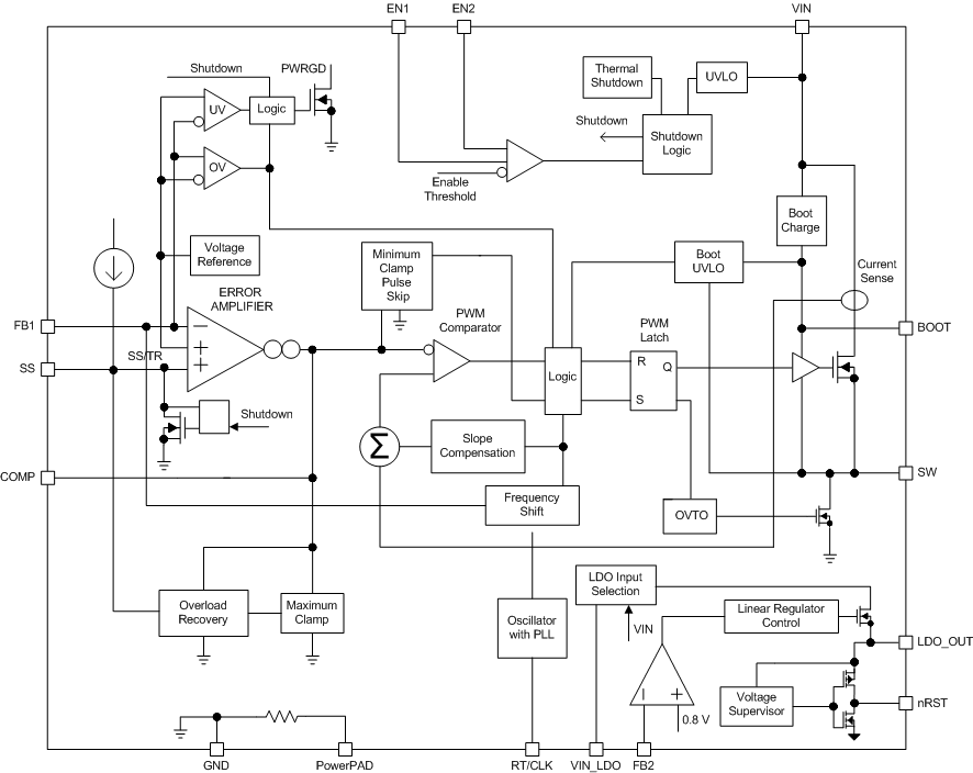
The TPS65320-Q1 buck regulator is a 40-V, 3.2-A, step-down (buck) converter with a 280-mA LDO linear regulator. Both regulators have low quiescent consumption during a light loads to prolong the battery life.
The buck converter improves performance during line and load transients by implementing a constant-frequency and current-mode control that reduces output capacitance, simplifying external frequency-compensation design. The wide switching frequency of 100 kHz to 2500 kHz allows for efficiency and size optimization when selecting the output-filter components. The switching frequency can be adjusted by using a resistor to ground on the RT/CLK pin. The buck converter has an internal phase-locked loop (PLL) on the RT/CLK pin that synchronizes the power switch turnon to the falling edge of an external system clock.
The TPS65320-Q1 buck regulator reduces the external component count by integrating the boot recharge diode. A capacitor between the BOOT and SW pins supplies the bias voltage for the integrated high-side MOSFET. The output voltage can be stepped down to as low as the 0.8-V reference. The soft-start feature minimizes inrush currents and provides power-supply sequencing during power up. Connect a small-value capacitor to the SS pin to adjust the soft-start time. Couple a resistor divider to the pin for critical power-supply sequencing requirements.
The LDO regulator only consumes about 40-µA current in light loads. The LDO regulator can also track the battery when battery voltage is low (in a cold-crank condition). The input of the LDO regulator has a unique auto-source feature which sources the input supply from either the buck output or the battery. If both the buck and LDO regulators are enabled, the buck regulator switches the input of the LDO regulator to the output of the buck to reduce heat. With the buck disabled or the buck output voltage out of regulation (VFB1 less than 91% of Vref), the buck regulator switches the LDO input automatically to the input voltage.
The LDO regulator of the TPS65320-Q1 device has a power-good comparator (nRST) that asserts when the regulated output voltage is less than 91% of the nominal output voltage.
7.2 Functional Block Diagram
7.3 Feature Description
7.3.1 Buck Regulator
7.3.1.1 Fixed-Frequency PWM Control
The TPS65320-Q1 buck regulator uses an adjustable, fixed-frequency peak-current mode control. An internal voltage reference compares the output voltage through external resistors on the FB1 pin to an error amplifier which drives the COMP pin. An internal oscillator initiates the turnon of the high-side power switch. The buck regulator compares the error amplifier output to the high-side power-switch current. When the power-switch current reaches the level set by the COMP voltage, the power switch turns off. The COMP pin voltage increases and decreases as the output current increases and decreases. The buck regulator implements a current limit by clamping the COMP pin voltage to a maximum level.
7.3.1.2 Slope Compensation Output
The TPS65320-Q1 buck regulator adds a compensating ramp to the switch current signal. This slope compensation prevents sub-harmonic oscillations. The available peak-inductor current remains constant over the full duty-cycle range.
7.3.1.3 Pulse-Skip Eco-mode™ Control Scheme
The TPS65320-Q1 buck regulator operates in a pulse-skip mode at light load currents to improve efficiency by reducing switching and gate-drive losses. The design of the TPS65320-Q1 buck regulator is such that if the output voltage is within regulation and the peak switch current at the end of any switching cycle is below the pulse-skipping-current threshold, the buck regulator enters pulse-skip mode. This current threshold is the current level corresponding to a nominal COMP voltage, or 720 mV. The current at which entry to the pulse-skip mode occurs depends on switching frequency, inductor selection, output-capacitor selection, and compensation network.
In pulse-skip mode, the buck regulator clamps the COMP pin voltage at 720 mV, inhibiting the high-side MOSFET. Further decreases in load current or in output voltage cannot drive the COMP pin below this clamp-voltage level. Because the buck regulator is not switching, the output voltage begins to decay. As the voltage-control loop compensates for the falling output voltage, the COMP pin voltage begins to rise. At this time, the high-side MOSFET turns on and a switching pulse initiates on the next switching cycle. The peak current is set by the COMP pin voltage. The output current recharges the output capacitor to the nominal voltage, then the peak switch current begins to decrease, and eventually falls below the pulse-skip-mode threshold, at which time the buck regulator enters Eco-mode again.
For pulse-skip-mode operation, the TPS65320-Q1 buck regulator senses the peak current, not the average or load current. Therefore, the load current where the buck regulator enters pulse-skip mode is dependent on the output inductor value. When the load current is low and the output voltage is within regulation, the buck regulator enters a sleep mode and draws only 140-µA input quiescent current. The internal PLL remains operating when the buck regulator is in sleep mode.
7.3.1.4 Dropout Operation and Bootstrap Voltage (BOOT)
The TPS65320-Q1 buck regulator has an integrated boot regulator and requires a small ceramic capacitor between the BOOT and SW pins to provide the gate-drive voltage for the high-side MOSFET. The BOOT capacitor recharges when the high-side MOSFET is off and the low-side diode conducts. The value of this ceramic capacitor should be 0.1 µF. TI recommends a ceramic capacitor with an X7R or X5R grade dielectric and a voltage rating of 10 V or higher because of the stable characteristics over temperature and voltage.
To improve drop out, the high-side MOSFET of the TPS65320-Q1 buck regulator remains on for 7 consecutive switching cycles, and is forced off during the 8th switching cycle to allow the low-side diode to conduct and refresh the charge on the BOOT capacitor. Because the current supplied by the BOOT capacitor is low, the high-side of the MOSFET can remain on longer before it is required to refresh the BOOT capacitor.
Voltage drops across the power MOSFET, inductor resistance, low-side diode, and printed circuit board resistance are the main influence on the effective duty cycle during dropout of the regulator. During operating conditions in which the input voltage drops and the regulator is operating in continuous-conduction mode (CCM), the high-side MOSFET can remain on for 100% of the duty cycle to maintain output regulation until the BOOT to SW voltage falls below 2.1 V.
Careful attention must be given to maximum duty cycle applications that experience extended time periods with light loads or no load. When the voltage across the BOOT capacitor falls below the 2.1-V UVLO threshold, the high-side MOSFET turns off, however not-enough inductor current exists to pull the SW pin down to recharge the BOOT capacitor. The high-side MOSFET of the regulator stops switching because the voltage across the BOOT capacitor is less than 2.1 V. The output capacitor then decays until the difference in the input voltage and output voltage is greater than 2.1 V, which exceeds the BOOT UVLO threshold, and the buck regulator begins switching again until reaching the desired output voltage. This operating condition persists until the input voltage, the load current, or both increase.
7.3.1.5 Error Amplifier
The buck converter of the TPS65320-Q1 buck regulator has a transconductance amplifier acting as the error amplifier. The error amplifier compares the FB1 voltage to the lower of the internal soft-start (SS) voltage or the internal 0.8-V voltage reference. The transconductance (gm) of the error amplifier is 310 µS during normal operation. During the soft-start operation, the transconductance is a fraction of the normal operating gm. When the voltage of the voltage on the FB1 pin is below 0.8 V and the buck regulator is regulating using an internal SS voltage, the gm is 70 µS. For frequency compensation, external compensation components (capacitor with series resistor and an optional parallel capacitor) must be connected between the COMP pin and the GND pin.
7.3.1.6 Voltage Reference
The voltage reference system produces a precise ±2% voltage reference over temperature by scaling the output of a temperature-stable bandgap circuit.
7.3.1.7 Adjusting the Output Voltage
A resistor divider from the output node to the FB1 pin sets the output voltage. Using a divider resistor with a tolerance of 1% or better is recommended. Begin with a value of 10 kΩ for the R2 resistor and use Equation 1 to calculate the value of R1. To improve efficiency at light loads, consider using larger-value resistors. If the values are too high, the regulator is more susceptible to noise and voltage errors from the FB1 input current are noticeable.

where
- VO is the buck regulator output voltage
7.3.1.8 Soft-Start and Tracking Pin (SS/TR)
The TPS65320-Q1 buck regulator effectively uses the lower voltage of the internal voltage reference or the SS/TR pin voltage as the reference voltage of the power supply and regulates the output accordingly. A capacitor on the SS/TR pin to ground implements a soft-start time. The TPS65320-Q1 buck regulator has an internal pullup-current source of 2 µA that charges the external soft-start capacitor. Use Equation 2 to calculate to calculate the value of the soft-start capacitor, CSS, which sets the soft-start time, tSS (10% to 90%). The soft-start capacitor should remain lower than 0.47 μF and greater than 1 nF.

where
- The voltage reference (Vref) is 0.8 V.
- The soft-start current (ISS) is 2 µA
At power up with the EN1 pin or after recovering from a UVLO event or from a thermal shutdown event, the TPS65320-Q1 buck regulator does not begin switching until the soft-start pin, SS/TR, discharges to less than 40 mV to ensure a proper power up.
7.3.1.9 Overload Recovery Circuit
The TPS65320-Q1 buck regulator has an overload recovery (OLR) circuit. The OLR circuit soft-starts the output from the overload voltage to the nominal regulation voltage on removal of the fault condition. The OLR circuit discharges the SS/TR pin to a voltage slightly greater than the FB1 pin voltage using an internal pulldown of 382 µA when the error amplifier changes to a high voltage from a fault condition. On removal of the fault condition, the output soft-starts from the fault voltage to the nominal output voltage.
7.3.1.10 Constant Switching Frequency and Timing Resistor (RT/CLK Pin)
The switching frequency of the TPS65320-Q1 buck regulator is adjustable over a wide range from approximately 100 kHz to 2500 kHz by placing a resistor on the RT/CLK pin. The RT/CLK pin voltage is typically 0.5 V and must have a resistor to ground to set the switching frequency. To determine the timing resistance for a given switching frequency, use Equation 3 or the curves in Figure 2. To reduce the solution size, the user typically sets the switching frequency as high as possible, but consider tradeoffs of the supply efficiency, maximum input voltage, and minimum controllable on-time. The minimum controllable on-time is typically 100 ns and limits the maximum operating input voltage. The frequency-shift circuit also limits the maximum switching frequency. The following sections discuss the maximum switching frequency in detail.

7.3.1.11 Overcurrent Protection and Frequency Shift
The TPS65320-Q1 buck regulator implements current mode control, which uses the COMP pin voltage to turn off the high-side MOSFET on a cycle-by-cycle basis. During each cycle, the switch current and COMP pin voltage are compared. When the peak switch current intersects the COMP voltage, the high-side switch turns off. During overcurrent conditions that pull the output voltage low, the error amplifier responds by driving the COMP pin high, increasing the switch current. Internal clamping of the error-amplifier output functions as a switch-current limit.
The TPS65320-Q1 buck regulator implements a frequency shift. The switching frequency is divided by 8, 4, 2, and 1 as the voltage ramps from 0 to 0.8 V on the FB1 pin. During short-circuit events (particularly with high-input-voltage applications), the control loop has a finite minimum controllable on-time, and the output has a low voltage. During the switch on-time, the inductor current ramps to the peak current limit because of the high input voltage and minimum on-time. During the switch off-time, the inductor would normally not have enough off time and output voltage for the inductor to ramp down by the ramp up amount. The frequency shift effectively increases the off-time, allowing the current to ramp down.
7.3.1.12 Selecting the Switching Frequency
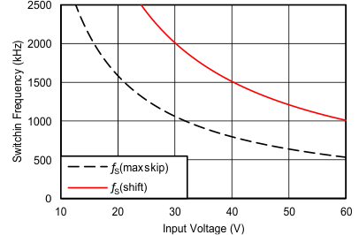
The switching frequency that is selected should be the lower value of the two equations, Equation 4 and Equation 5. Use Equation 4 to calculate the maximum switching frequency limitation set by the minimum controllable on-time. Setting the switching frequency above this value causes the regulator to skip switching pulses. The buck regulator maintains regulation, but pulse-skipping leads to high inductor current and a significant increase in output ripple voltage.
Use Equation 5 to calculate the maximum switching frequency limit set by the frequency-shift protection. For adequate output short-circuit protection at high input voltages, set the switching frequency to a value less than the ƒS(maxshift) frequency. In Equation 5, to calculate the maximum switching frequency one must take into account that the output voltage decreases from the nominal voltage to 0 volts, and the ƒdiv integer increases from 1 to 8 corresponding to the frequency shift.
In Figure 8, the solid line illustrates a typical safe operating area regarding frequency shift and assumes the output voltage is zero volts, the resistance of the inductor is 0.130 Ω, the FET on-resistance is 0.127 Ω, and the diode voltage drop is 0.5 V. The dashed line is the maximum switching frequency to avoid pulse skipping.

where
- tON = controllable on-time (typ. 100 ns)
- IL = inductor current
- RDC = inductor resistance
- VO = output voltage
- Vd = diode voltage drop
- VI = maximum input voltage
- RHS = FET on resistance (127 mΩ typical)

where
- ƒdiv = frequency divide factor (equals 8, 4, 2 or 1)
- VO(SC) = output voltage during short
| IL = 1 A | VO = 3.3 V |
7.3.1.13 How to Interface to RT/CLK Pin
The RT/CLK pin synchronizes the buck regulator to an external system clock. To implement the synchronization feature, connect a square wave to the RT/CLK pin through the circuit network shown in Figure 9. The square-wave amplitude must transition lower than 0.5 V and higher than 2.2 V on the RT/CLK pin and have an on-time greater than 40 ns and an off-time greater than 40 ns. The synchronization frequency range is 300 kHz to 2200 kHz. The rising edge of SW is synchronizes with the falling edge of RT/CLK pin signal. Design the external synchronization circuit in such a way that the buck regulator has the default frequency-set resistor connected from the RT/CLK pin to ground should the synchronization signal turn off. Using a frequency-set resistor connected as shown in Figure 9 through a 50-Ω resistor to ground is recommended. The resistor should set the switching frequency close to the external CLK frequency. TI also recommends AC-coupling the synchronization signal through a 10-pF ceramic capacitor to the RT/CLK pin and a 4-kΩ series resistor. The series resistor reduces SW jitter in heavy-load applications when synchronizing to an external clock, and in applications which transition from synchronizing to RT mode. The first time CLK is pulled above the CLK threshold, the buck regulator switches from the RT resistor frequency to PLL mode. Along with the resulting removal of the internal 0.5-V voltage source, the CLK pin becomes high-impedance as the PLL begins to lock onto the external signal. Because regulator has a PLL, the switching frequency can be higher or lower than the frequency set with the external resistor. The buck regulator transitions from the resistor mode to the PLL mode and then increases or decreases the switching frequency until the PLL locks onto the CLK frequency within 100 ms.
When the buck regulator transitions from the PLL mode to the resistor mode, the switching frequency slows down from the CLK frequency to 150 kHz, then reapplies the 0.5-V voltage. the resistor then sets the switching frequency. The switching-frequency divisor changes to 8, 4, 2, and 1 as the voltage ramps from 0 to 0.8 V on the FB1 pin. The buck regulator implements a digital frequency shift to enable synchronizing to an external clock during normal startup and fault conditions.
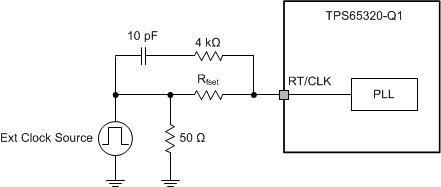 Figure 9. Synchronizing to a System Clock
7.3.1.14 Overvoltage Transient Protection
The TPS65320-Q1 buck regulator incorporates an overvoltage transient-protection (OVTP) circuit to minimize voltage overshoot when recovering from output fault conditions or strong unload transients on power-supply designs with low-value output capacitance. For example, with the power-supply output overloaded, the error amplifier compares the actual output voltage to the internal reference voltage. If the FB1 pin voltage is lower than the internal reference voltage for a considerable time, the output of the error amplifier responds by clamping the error amplifier output to a high voltage, thus requesting the maximum output current. On removal of the condition, the regulator output rises and the error-amplifier output transitions to the steady-state duty cycle. In some applications, the power-supply output voltage can respond faster than the error-amplifier output can respond which actuality leads to the possibility of an output overshoot. The OVTP feature minimizes the output overshoot when using a low-value output capacitor by implementing a circuit to compare the FB1 pin voltage to the OVTP threshold (which is 109% of the internal voltage reference). The FB1 pin voltage going higher than the OVTP threshold disables the high-side MOSFET, preventing current from flowing to the output and minimizing output overshoot. The FB1 voltage dropping lower than the OVTP threshold allows the high-side MOSFET to turn on at the next clock cycle.
7.3.1.15 Thermal Shutdown
The buck regulator implements an internal thermal shutdown to protect the regulator if the junction temperature exceeds 155°C (typical). The thermal shutdown forces the buck regulator to stop switching when the junction temperature exceeds the thermal trip threshold. When the junction temperature decreases below 145°C (typical), the buck regulator reinitiates the power-up sequence.
7.3.1.16 Small-Signal Model for Loop Response
Figure 10 shows an equivalent model for the TPS65320-Q1 control loop which can be modeled in a circuit-simulation program to check frequency response and dynamic load response. The error amplifier is a transconductance amplifier with a gmea of μA/V. One can model the error amplifier using an ideal voltage-controlled current source. Resistor Ro and capacitor Co model the open-loop gain and frequency response of the amplifier. The 1-mV AC voltage source between nodes a and b effectively breaks the control loop for the frequency-response measurements. Plotting c versus a shows the small signal response of the frequency compensation. Plotting a versus b shows the small signal response of the overall loop. Check the dynamic loop response by replacing RL with a current source that has the appropriate load-step amplitude and step rate in a time-domain analysis. This equivalent model is only valid for continuous-conduction-mode designs.
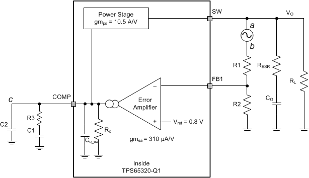 Figure 10. Small-Signal Model for Loop Response
7.3.1.17 Simple Small-Signal Model for Peak-Current Mode Control
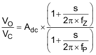
Figure 11 shows a simple small-signal model that can be used to understand how to design the frequency compensation. A voltage-controlled current source (duty cycle modulator) supplying current to the output capacitor and load resistor can approximate the buck-regulator power stage. Equation 6 shows the control-to-output transfer function, which consists of a DC gain, one dominant pole, and one ESR zero. The quotient of the change in switch current divided by the change in COMP pin voltage (node c in Figure 10) is the power-stage transconductance. The gmPS for the buck-regulator power stage buck regulator is 10.5 A/V. Use Equation 7 to calculate the low-frequency gain of the power stage which is the product of the transconductance and the load resistance.
As the load current increases and decreases, the low-frequency gain decreases and increases, respectively. This variation with the load may seem problematic at first, but the dominant pole moves with the load current (see Equation 8). The dashed line in the right half of Figure 11 highlights the combined effect. As the load current decreases, the gain increases and the pole frequency lowers, keeping the 0-dB crossover frequency the same for the varying load conditions, which makes designing the frequency compensation easier. The type of selected output capacitor determines whether the ESR zero has a profound effect on the frequency compensation design. Using high-ESR aluminum electrolytic capacitors can reduce the number of frequency-compensation components required to stabilize the overall loop because the phase margin increases from the ESR zero at the lower frequencies (see Equation 9).
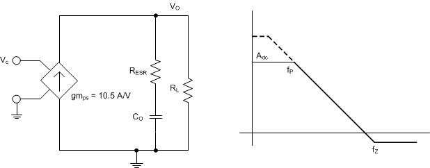 Figure 11. Simple Small-Signal Model and Frequency Response for Peak-Current Mode


7.3.1.18 Small-Signal Model for Frequency Compensation
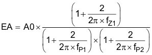
The buck regulator of the TPS65320-Q1 device uses a transconductance amplifier for the error amplifier. Figure 12 shows compensation circuits. Implementation of Type 2 circuits is most likely in high-bandwidth power-supply designs. The purpose of loop compensation is to ensure stable operation while maximizing dynamic performance. Use of the Type 1 circuit is with power-supply designs that have high-ESR aluminum electrolytic or tantalum capacitors. Equation 10 and Equation 11 show how to relate the frequency response of the amplifier to the small-signal model in Figure 12. Modeling of the open-loop gain and bandwidth uses the Ro and Co shown in Figure 12. See the Typical Applications section for a design example with a Type 2A network that has a low-ESR output capacitor. For stability purposes, the target is to have a loop-gain slope that is –20 dB/decade at the crossover frequency. Also, the crossover frequency should not exceed one-fifth of the switching frequency (120 kHz in the case of a 600-kHz switching frequency).
For dynamic purposes, the higher the bandwidth, the faster the load-transient response. A large DC gain means high DC regulation accuracy (DC voltage changes little with load or line variations). To achieve this loop gain, set the compensation components according to the shape of the control-output bode plot.
Equation 10 through Equation 20 serve as a reference to calculate the compensation components. Ro and C1 form the dominant pole (P1). A resistor (R3) and a capacitor (C1) in series to ground work as zero (Z1). In addition, for an optional pole, add a lower-value capacitor (C2) in parallel with R3 to. This capacitor can be used to filter noise at switching frequency, and it is also needed if the output capacitor has high ESR.
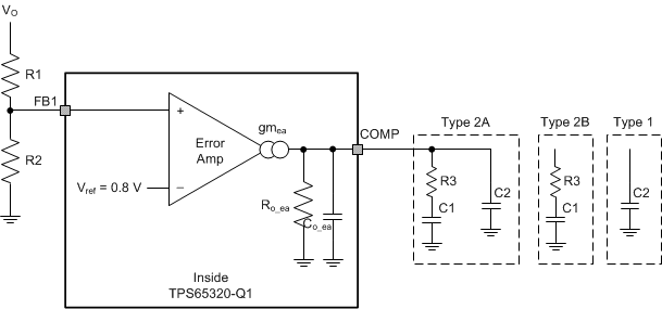 Figure 12. Types of Frequency Compensation
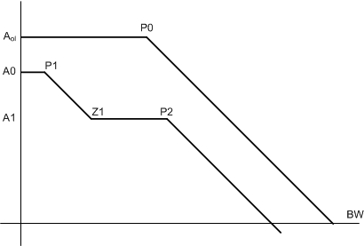 Figure 13. Frequency Response of the Type 2 Frequency Compensation




7.3.2 LDO Regulator
For the TPS65320-Q1 device, the design of the linear regulator is for low-power consumption and a quiescent current of about 40 µA in light-load applications.
The LDO regulator requires both supplies from VIN and VIN_LDO to function. At all times the voltage level of VIN must be higher or equal to the voltage level of VIN_LIN for the the LDO regulator to function properly. The current capability of the LDO regulator is 280 mA under the full VIN_LDO input range, while VIN ≥ 4 V. When VIN becomes less than 4 V, the current capability of the LDO regulator decreases.
7.3.2.1 Charge-Pump Operation
The LDO regulator has an internal charge pump which turns on or off depending on the input voltage. The charge-pump switching circuitry does not cause conducted emissions to exceed required thresholds on the input voltage line. The charge-pump switching thresholds are hysteretic. Figure 14 shows the typical switching thresholds for the charge pump.
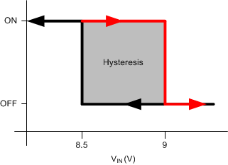 Figure 14. Charge-Pump Switching Thresholds
Table 1. Typical Quiescent Current Consumption
| CHARGE PUMP ON | CHARGE PUMP OFF | |
|---|---|---|
| LDO Iq | 300 µA | 40 µA |
7.3.2.2 Low-Voltage Tracking
At low input voltages, the regulator drops out of regulation, and the output voltage tracks input minus a dropout voltage (VDROPOUT). This feature allows for a smaller input capacitor and can possibly eliminate the requirement for a boost convertor during cold-crank conditions.
7.3.2.3 Power-Good Output, nRST
The nRST pin is a push-pull output formed by a push-pull stage between LDO_OUT and GND pins. The power-on-reset output asserts low until the output voltage on LDO_OUT exceeds the setting thresholds (91%) and the deglitch timer has expired. Additionally, whenever the EN2 pin is low or open, the nRST pin immediately asserts low regardless of the output voltage. If a thermal shutdown occurs because of excessive thermal conditions, this pin also asserts low. When the nRST is released (not asserted low), it can only be pulled-up to the specified VOH voltage when the LDO_OUT voltage is equal to or higher than 3.3 V.
7.3.3 Enable and Undervoltage Lockout
The TPS65320-Q1 device enable pins (EN1 and EN2) are high-voltage-tolerant input pins with an internal pulldown circuit. A high input activates the buck regulator and turns the regulators ON.
The TPS65320-Q1 device has an internal UVLO circuit to shut down the output if the input voltage falls below an internally fixed UVLO threshold level. This UVLO circuit ensures that both regulators are not latched into an unknown state during low-input-voltage conditions. The regulators power up when the input voltage exceeds the voltage level.
7.4 Device Functional Modes
7.4.1 Modes of Operation
The buck regulator has two hardware enable pins, and one can turn off either the buck or the LDO by pulling the enable pin low, as listed in Table 2. One unique feature of the TPS65320-Q1 buck regulator is the input auto source of the LDO. With both the buck and the LDO enabled, the LDO receives input from the output of the buck through the VIN_LDO pin. In this mode, the buck output voltage must be higher than the LDO output voltage. With the buck disabled and the LDO still enabled, the input of the LDO changes automatically from VIN_LDO to VIN which is useful for standby operations which need a very low standby current, such as automotive infotainment, telematics, and other operations. The LDO changes the input when the buck output voltage is out of regulation (V(FB1) is less than 91% of Vref1).
Table 2. Device Operation Modes
| BUCK | LDO | DESCRIPTION |
|---|---|---|
| EN1 | EN2 | |
| 0 | 0 | Both buck and LDO disabled |
| 0 | 1 | Buck disabled. LDO enabled and LDO input source is from the battery. |
| 1 | 0 | Buck enabled and LDO disabled |
| 1 | 1 | Both buck and LDO enabled and LDO input source is from buck output. Buck output voltage must be higher than LDO output voltage. |
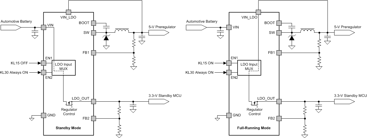 Figure 15. Example of LDO Auto Source in Standby Condition