ZHCSG38A March 2017 – November 2022 TPS65263-1Q1
PRODUCTION DATA
- 1 特性
- 2 应用
- 3 说明
- 4 Revision History
- 5 Pin Configuration and Functions
- 6 Specifications
-
7 Detailed Description
- 7.1 Overview
- 7.2 Functional Block Diagram
- 7.3
Feature Description
- 7.3.1 Adjusting the Output Voltage
- 7.3.2 Enable and Adjusting UVLO
- 7.3.3 Soft-Start Time
- 7.3.4 Power-Up Sequencing
- 7.3.5 V7V Low-Dropout Regulator and Bootstrap
- 7.3.6 Out-of-Phase Operation
- 7.3.7 Output Overvoltage Protection (OVP)
- 7.3.8 PSM
- 7.3.9 Slope Compensation
- 7.3.10 Overcurrent Protection
- 7.3.11 Power Good
- 7.3.12 Thermal Shutdown
- 7.4 Device Functional Modes
- 7.5 Register Maps
- 8 Application and Implementation
- 9 Device and Documentation Support
- 10Mechanical, Packaging, and Orderable Information
8.2.2.4 Loop Compensation
The TPS65263-1Q1 incorporates a peak current mode control scheme. The error amplifier is a transconductance amplifier with a gain of 300 µS. A typical type II compensation circuit adequately delivers a phase margin between 40° and 90°. Cb adds a high-frequency pole to attenuate high-frequency noise when needed. To calculate the external compensation components, follow these steps.
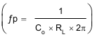
- Select switching frequency, ƒsw, that is appropriate for application depending on L and C sizes, output ripple, EMI, and so forth. Switching frequency between 500 kHz to 1 MHz gives best trade-off between performance and cost. To optimize efficiency, lower switching frequency is desired.
- Set up crossover frequency, ƒc, which is typically between 1/5 and 1/20 of ƒsw.
- RC can be determined by:
Equation 18.
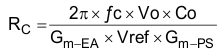
where
- Gm_EA is the error amplifier gain (300 µS).
- Gm_PS is the power stage voltage to current conversion gain (7.4 A/V).
- Calculate CC by placing a compensation zero at or before the dominant pole
 .
Equation 19.
.
Equation 19.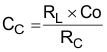
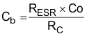
- Optional Cb can be used to cancel the zero from the ESR associated with CO.
Equation 20.
- Type III compensation can be implemented with the addition of one capacitor, C1. This allows for slightly higher loop bandwidths and higher phase margins. If used, calculate C1 from Equation 21.
Equation 21.
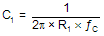
 Figure 8-2 DC/DC Loop Compensation