ZHCSG38A March 2017 – November 2022 TPS65263-1Q1
PRODUCTION DATA
- 1 特性
- 2 应用
- 3 说明
- 4 Revision History
- 5 Pin Configuration and Functions
- 6 Specifications
-
7 Detailed Description
- 7.1 Overview
- 7.2 Functional Block Diagram
- 7.3
Feature Description
- 7.3.1 Adjusting the Output Voltage
- 7.3.2 Enable and Adjusting UVLO
- 7.3.3 Soft-Start Time
- 7.3.4 Power-Up Sequencing
- 7.3.5 V7V Low-Dropout Regulator and Bootstrap
- 7.3.6 Out-of-Phase Operation
- 7.3.7 Output Overvoltage Protection (OVP)
- 7.3.8 PSM
- 7.3.9 Slope Compensation
- 7.3.10 Overcurrent Protection
- 7.3.11 Power Good
- 7.3.12 Thermal Shutdown
- 7.4 Device Functional Modes
- 7.5 Register Maps
- 8 Application and Implementation
- 9 Device and Documentation Support
- 10Mechanical, Packaging, and Orderable Information
7.3.2 Enable and Adjusting UVLO
The ENx pin provides electrical on and off control of the device. After the ENx pin voltage exceeds the threshold voltage, the device starts operation. If each ENx pin voltage is pulled below the threshold voltage, the regulator stops switching and enters a low Iq state.
The EN pin has an internal pullup current source, allowing the user to float the EN pin for enabling the device. If an application requires controlling the EN pin, use open-drain or open-collector output logic to interface with the pin.
The device implements internal UVLO circuitry on the VIN pin. The device is disabled when the VIN pin voltage falls below the internal VIN UVLO threshold. The internal VIN UVLO threshold has a hysteresis of 500 mV. If an application requires either a higher UVLO threshold on the VIN pin or a secondary UVLO on the PVINx in split rail applications, then the user can configure the ENx pin as shown in Figure 7-3, Figure 7-4, and Figure 7-5. When using the external UVLO function, TI recommends to set the hysteresis >500 mV.
The EN pin has a small pullup current, Ip, which sets the default state of the pin to enable when no external components are connected. The pullup current is also used to control the voltage hysteresis for the UVLO function because it increases by Ih after the EN pin crosses the enable threshold. The UVLO thresholds can be calculated using Equation 2 and Equation 3.
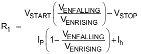
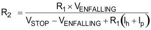
where
- Ih = 3 µA
- Ip = 3.9 µA
- VENRISING = 1.2 V
- VENFALLING = 1.15 V
 Figure 7-3 Adjustable VIN UVLO
 Figure 7-5 Adjustable VIN and PVIN UVLO
 Figure 7-4 Adjustable PVIN UVLO, VIN > 4 V